

| Distributor | Stock | Pricing | MOQ | PKG | Lead Time | Date Code | On Order Quantity | On Order Delivery | |
|---|---|---|---|---|---|---|---|---|---|
|
6,873 pcs
|
6873 pcs | On Request | 1 | On Request | On Request | On Request | On Request | On Request |
| Category | |
| Manufacturer Name | |
| Differential | |
| Frequency | |
| Input | |
| Input Type | |
| Mounting Type | |
| Number of Circuits | |
| Operating Temperature | |
| Output | |
| Ratio | |
| Storage Temperature | |
| Supplier Device Package | |
| Supplier Package | |
| Tape & Reel | |
| Type | |
| Voltage |
The NB3V1102CMTTBG from On Semiconductor is a modular, high-performance, low-skew, general-purpose LVCMOS clock buffer. Designed for flexibility, it offers a 1:2 fanout configuration and operates across a wide supply voltage range from 1.71V to 3.6V.
This device boasts a maximum operating frequency of 250 MHz, making it suitable for various timing applications. It maintains very low output-to-output skew, less than 50 ps, and very low additive jitter, less than 200 fs, ensuring signal integrity. The operating temperature range is specified from -40°C to 105°C (TA).
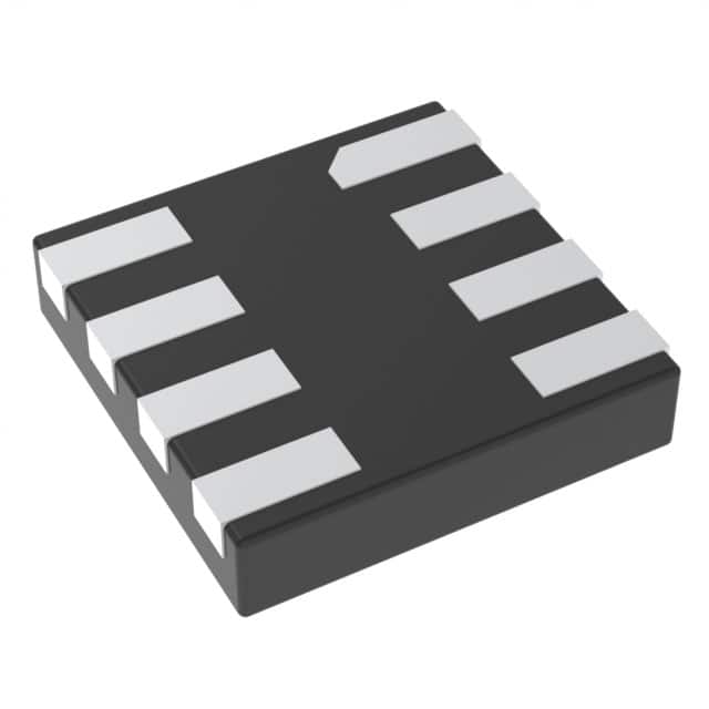
The NB3V1102CMTTBG supports an asynchronous output enable control (OE) which switches the outputs to a low state when OE is low. It is available in an 8-WDFN (2x2) surface-mount package, facilitating integration into compact designs.
Key electrical characteristics include LVCMOS input and output types, and it is designed as a single circuit buffer. The device is RoHS3 compliant and has a Moisture Sensitivity Level (MSL) of 1.
| Qty | Low | High |
|---|---|---|
| 1+ | $4.44 | $4.44 |
Estimated market price range - modelled values for guidance only, not live distributor offers.
The operating voltage range is 1.71V to 3.6V.
The maximum frequency is 250 MHz.
The operating temperature range is -40°C to 105°C.
It is available in an 8-WDFN (2x2) package.
The output skew is less than 50 ps.
The additive jitter is less than 200 fs.