

| Distributor | Stock | Pricing | MOQ | PKG | Lead Time | Date Code | On Order Quantity | On Order Delivery | |
|---|---|---|---|---|---|---|---|---|---|
|
6,413 pcs
|
6413 pcs | On Request | 1 | On Request | On Request | On Request | On Request | On Request |
| Category | |
| Manufacturer Name | |
| Differential | |
| Frequency | |
| Input | |
| Lead Spacing | |
| Mounting Type | |
| Number of Circuits | |
| Operating Temperature | |
| Output | |
| Pitch | |
| Ratio | |
| Supplier Device Package | |
| Type | |
| Voltage |
The NB3RL02FCT2G from On Semiconductor is a two-channel clock fanout buffer designed for low-skew and low-jitter applications. It is ideal for portable equipment such as mobile phones.
This buffer supports a master clock input and provides two clock outputs, controlled by CLK_REQ1 and CLK_REQ2 inputs. It operates with an input voltage range of 2.3 V to 5.5 V and can handle frequencies up to 80 MHz, with a typical operating frequency of 52 MHz. The device features adaptive clock output buffers that minimize EMI emissions and maintain signal integrity.
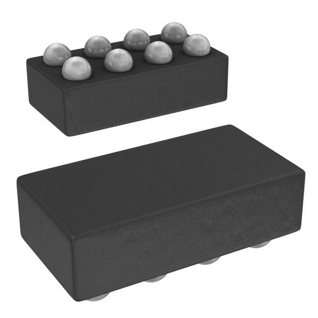
An integrated Low-Drop-Out (LDO) voltage regulator provides a regulated 1.8 V output, which can be used to power external clock sources like TCXOs. The NB3RL02FCT2G is offered in an ultra-small 8-ball Wafer-Level Chip Scale Package (WLCS) with a 0.4 mm pitch, optimized for very low standby current consumption.
Key electrical characteristics include low additive noise of -149 dBc/Hz at 10 kHz offset and output jitter of 0.37 ps (rms). It also meets stringent ESD performance requirements, exceeding JESD 22 standards for Human-Body Model, Machine Model, and Charged-Device Model.
The NB3RL02FCT2G is suitable for applications in cellular phones and Global Positioning Systems (GPS). It is mounted using a surface mount technique and operates within a temperature range of -40°C to 85°C.
| Qty | Low | High |
|---|---|---|
| 1+ | $4.44 | $4.44 |
Estimated market price range - modelled values for guidance only, not live distributor offers.
The operating voltage range for the NB3RL02FCT2G is 2.3 V to 5.5 V.
The output jitter of the NB3RL02FCT2G is 0.37 ps (rms).
The operating temperature range for the NB3RL02FCT2G is -40°C to 85°C.
The NB3RL02FCT2G is supplied in an 8-ball Wafer-Level Chip Scale Package (WLCS) with a 0.4 mm pitch.
Yes, the NB3RL02FCT2G has an integrated Low-Drop-Out (LDO) voltage regulator that outputs 1.8 V.
The RoHS status of the NB3RL02FCT2G is RoHS3 Compliant.