

| Distributor | Stock | Pricing | MOQ | PKG | Lead Time | Date Code | On Order Quantity | On Order Delivery | |
|---|---|---|---|---|---|---|---|---|---|
|
45,000 pcs
|
45000 pcs | On Request | 1 | On Request | On Request | On Request | On Request | On Request |
| Category | |
| Manufacturer Name | |
| AEC Qualified | |
| Automotive Grade | |
| Differential | |
| Frequency | |
| Industrial Grade | |
| Input | |
| Input Type | |
| Medical Grade | |
| Military Grade | |
| Mounting Type | |
| Number of Circuits | |
| Operating Temperature | |
| Output | |
| Propagation Delay | |
| Ratio | |
| Supplier Device Package | |
| Supplier Package | |
| Tape & Reel | |
| Type | |
| Voltage |
The NB3N853531EDTR2G is a low-skew, 3.3V supply clock distribution fanout buffer from ON Semiconductor. This device features a 2:1 input multiplexer that selects between a crystal oscillator or an LVCMOS/LVTTL clock source via the CLK_SEL pin. The selected input is then translated to four differential 3.3V LVPECL outputs.
With a maximum clock operation frequency of 266 MHz, the NB3N853531EDTR2G is suitable for high-speed clock distribution applications. It boasts low output-to-output skew of 30 ps (max) and device-to-device skew of 200 ps (max), ensuring signal integrity. The propagation delay is a maximum of 1.8 ns.
A synchronous clock enable control (CLK_EN) allows for disabling the outputs to eliminate runt pulses, operating with LVCMOS/LVTTL levels. The device operates within a voltage range of 3.135V to 3.465V and is specified for an industrial temperature range of -40°C to 85°C.
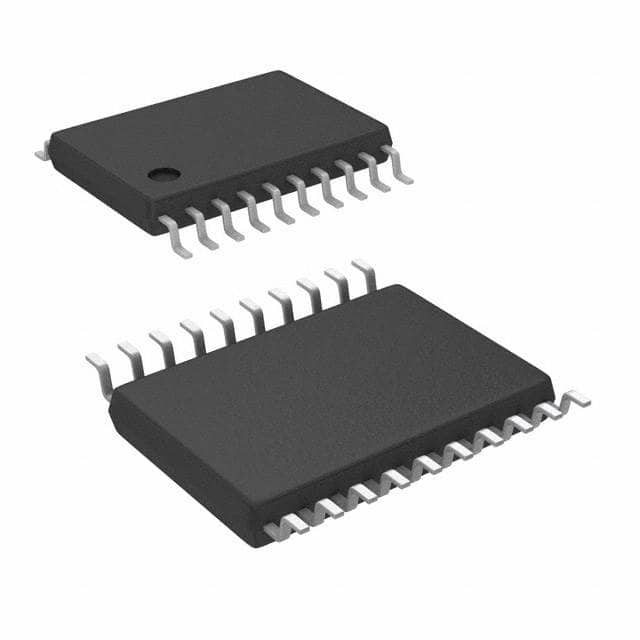
Packaged in a 20-TSSOP, the NB3N853531EDTR2G is designed for surface mount applications. It is Pb-free and RoHS compliant.
| Qty | Low | High |
|---|---|---|
| 1+ | $4.44 | $4.44 |
Estimated market price range - modelled values for guidance only, not live distributor offers.
The operating voltage for the NB3N853531EDTR2G is 3.3V ±5%, ranging from 3.135V to 3.465V.
The NB3N853531EDTR2G supports clock operation up to 266 MHz.
The NB3N853531EDTR2G features four differential 3.3V LVPECL outputs.
The device operates in an industrial temperature range from -40°C to 85°C.
The NB3N853531EDTR2G is supplied in a 20-TSSOP package.