

| Distributor | Stock | Pricing | MOQ | PKG | Lead Time | Date Code | On Order Quantity | On Order Delivery | |
|---|---|---|---|---|---|---|---|---|---|
|
8,990 pcs
|
8990 pcs | On Request | 1 | On Request | On Request | On Request | On Request | On Request |
| Category | |
| Manufacturer Name | |
| Differential | |
| Divider | |
| Frequency | |
| Input | |
| Lead Spacing | |
| Mounting Type | |
| Number of Circuits | |
| Operating Temperature | |
| Output | |
| PLL | |
| Phase Jitter | |
| Ratio | |
| Supplier Device Package | |
| Supplier Package | |
| Tape & Reel | |
| Voltage |
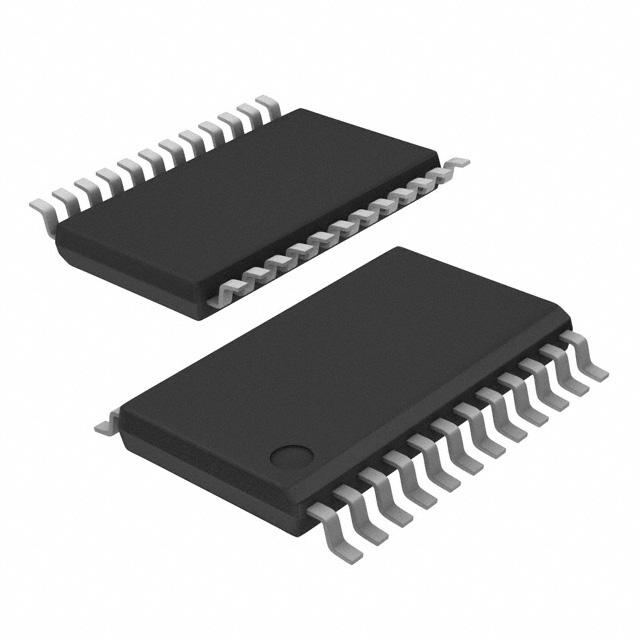
The NB3N51054DTR2G from ON Semiconductor is a high-performance clock generator designed for applications requiring precise clock signals, particularly those supporting PCI Express Gen 1 through Gen 4.
This device accepts a 25 MHz fundamental mode crystal or reference clock input and generates four differential HCSL or LVDS outputs operating at 100 MHz. It features low phase jitter of 0.5 ps and low cycle-cycle jitter of 20 ps, ensuring signal integrity. The generator supports selectable spread spectrum options (-0.35%, -0.5%) for reduced EMI, along with an option for no spread for optimal performance.
Control of individual outputs, including enabling and disabling them, is managed via an I2C interface, which also provides read-back capability. The NB3N51054DTR2G operates from a 3.3V supply with a ±5% tolerance and is rated for an industrial temperature range of -40°C to 85°C.
Packaged in a 24-TSSOP, this clock generator is suitable for surface mount applications. Its features make it ideal for networking, computing, consumer electronics, and industrial equipment requiring reliable PCIe clock generation.
| Qty | Low | High |
|---|---|---|
| 1+ | $7.01 | $7.01 |
Estimated market price range - modelled values for guidance only, not live distributor offers.
The NB3N51054DTR2G outputs a clock frequency of 100 MHz.
The NB3N51054DTR2G provides four differential HCSL or LVDS outputs.
The typical phase jitter for the NB3N51054DTR2G at 100 MHz is 0.5 ps.
The NB3N51054DTR2G operates at 3.3V with a tolerance of ±5%.
The operating temperature range for the NB3N51054DTR2G is -40°C to 85°C.
The NB3N51054DTR2G is supplied in a 24-TSSOP package.