

| Distributor | Stock | Pricing | MOQ | PKG | Lead Time | Date Code | On Order Quantity | On Order Delivery | |
|---|---|---|---|---|---|---|---|---|---|
|
31,000 pcs
|
31000 pcs | On Request | 1 | On Request | On Request | On Request | On Request | On Request |
| Category | |
| Manufacturer Name | |
| AEC Qualified | |
| Automotive Grade | |
| Differential | |
| Frequency | |
| Industrial Grade | |
| Input | |
| Medical Grade | |
| Military Grade | |
| Mounting Type | |
| Number of Circuits | |
| Operating Temperature | |
| Operating Voltage | |
| Output | |
| Propagation Delay | |
| Ratio | |
| Supplier Device Package | |
| Supplier Package | |
| Tape & Reel | |
| Type | |
| Voltage |
The NB3N111KMNR4G from On Semiconductor is a differential clock fanout buffer designed for applications requiring low propagation delay variation. It supports input frequencies up to 400 MHz and offers a 1:10 fanout ratio.
This buffer is optimized for PCI Express HCSL clock distribution and FBDIMM applications. It can accept various differential input signals including LVPECL, LVDS, and HCSL, as well as single-ended signals with an external reference. The outputs are HCSL, with optional LVDS output levels available when interface termination is used. The device operates within a voltage range of 3.0 V to 3.6 V and has an operating temperature range of -40°C to 85°C.
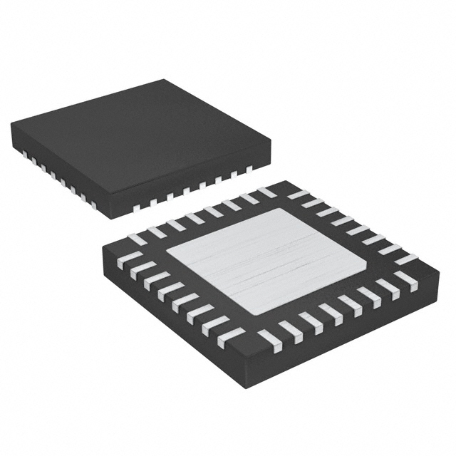
The NB3N111KMNR4G is available in a 32-VFQFN exposed pad package, suitable for surface mounting. It is designed to minimize output-to-output skew, making it ideal for distributing low-skew clocks across backplanes or motherboards.
| Qty | Low | High |
|---|---|---|
| 1+ | $4.44 | $4.44 |
Estimated market price range - modelled values for guidance only, not live distributor offers.
The operating voltage range is 3.0 V to 3.6 V.
It is available in a 32-VFQFN exposed pad package.
The operating temperature range is -40°C to 85°C.
The RoHS status is RoHS3 Compliant.