

| Distributor | Stock | Pricing | MOQ | PKG | Lead Time | Date Code | On Order Quantity | On Order Delivery | |
|---|---|---|---|---|---|---|---|---|---|
|
84,000 pcs
|
84000 pcs | On Request | 1 | On Request | On Request | On Request | On Request | On Request |
| Category | |
| Manufacturer Name | |
| Differential | |
| Frequency | |
| Input | |
| Input Capacitance | |
| Input Type | |
| Mounting Type | |
| Number of Circuits | |
| Operating Temperature | |
| Output | |
| Ratio | |
| Supplier Device Package | |
| Supplier Package | |
| Tape & Reel | |
| Type | |
| Voltage |
The ON Semiconductor NB3M8302CDR2G is a high-performance 1:2 fanout buffer designed for clock distribution applications. It accepts LVCMOS/LVTTL input levels and provides two LVCMOS/LVTTL outputs, making it suitable for a wide range of digital systems.
This buffer supports core supply voltages of 3.3V and output supply voltages of either 2.5V or 3.3V. It can operate at input clock frequencies up to 200 MHz with low output-to-output skew of 25 ps typical and part-to-part skew of 250 ps typical. The device is qualified for industrial operating temperature ranges from -40°C to +85°C.
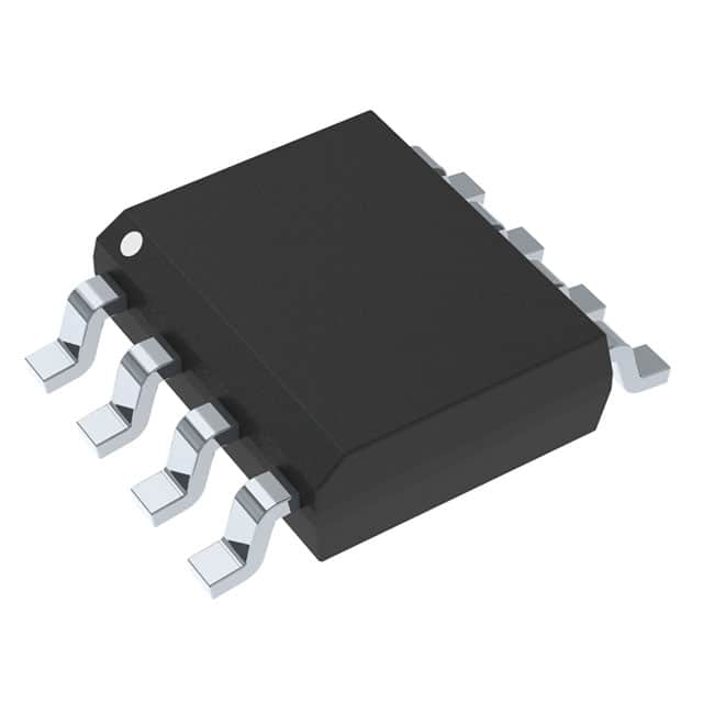
The NB3M8302CDR2G is housed in a standard 8-SOIC package, designed for surface mount applications. Its robust design and reliable performance make it a suitable choice for clock buffering and distribution needs in various electronic designs.
| Qty | Low | High |
|---|---|---|
| 1+ | $4.44 | $4.44 |
Estimated market price range - modelled values for guidance only, not live distributor offers.
The maximum input clock frequency is 200 MHz.
The device supports LVCMOS/LVTTL input and output logic levels.
The core supply voltage is 3.3V ±5%, and the output supply voltage can be 3.3V ±5% or 2.5V ±5%.
The operating temperature range is -40°C to +85°C.
The NB3M8302CDR2G is available in an 8-SOIC package.
Yes, the NB3M8302CDR2G is RoHS3 compliant.
The Moisture Sensitivity Level is 1.