

| Distributor | Stock | Pricing | MOQ | PKG | Lead Time | Date Code | On Order Quantity | On Order Delivery | |
|---|---|---|---|---|---|---|---|---|---|
|
14,850 pcs
|
14850 pcs | On Request | 1 | On Request | On Request | On Request | On Request | On Request |
| Category | |
| Manufacturer Name | |
| Differential | |
| Frequency | |
| Input | |
| Lead Spacing | |
| Mounting Type | |
| Number of Circuits | |
| Operating Temperature | |
| Output | |
| Ratio | |
| Supplier Device Package | |
| Tape & Reel | |
| Type | |
| Voltage |
The ON Semiconductor NB3L8533DTR2G is a high-performance clock buffer and multiplexer designed for clock distribution applications. This device features a single circuit capable of buffering and distributing clock signals with a frequency of up to 650 MHz.
It supports a wide range of input types including CML, HCSL, HSTL, LVDS, LVPECL, and SSTL, with an LVPECL output. The operating voltage range is from 2.375V to 3.63V, making it suitable for various system designs. The buffer provides a 2:4 ratio, enabling efficient signal fanout.
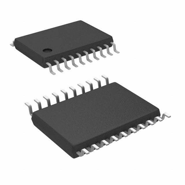
Designed for surface mounting, the NB3L8533DTR2G is housed in a compact 20-TSSOP package. It operates reliably within an ambient temperature range of -40°C to 85°C. The terminal finish is Nickel/Palladium/Gold (Ni/Pd/Au), ensuring good connectivity and durability.
| Qty | Low | High |
|---|---|---|
| 1+ | $4.44 | $4.44 |
Estimated market price range - modelled values for guidance only, not live distributor offers.
The NB3L8533DTR2G operates at a frequency of 650 MHz.
The operating voltage range for this clock buffer is 2.375V to 3.63V.
The NB3L8533DTR2G is supplied in a 20-TSSOP package.
This component operates within a temperature range of -40°C to 85°C.
The NB3L8533DTR2G requires surface mounting.