

| Distributor | Stock | Pricing | MOQ | PKG | Lead Time | Date Code | On Order Quantity | On Order Delivery | |
|---|---|---|---|---|---|---|---|---|---|
|
38,175 pcs
|
38175 pcs | On Request | 1 | On Request | On Request | On Request | On Request | On Request |
| Category | |
| Manufacturer Name | |
| Differential | |
| Frequency | |
| Input | |
| Lead Spacing | |
| Mounting Type | |
| Number of Circuits | |
| Operating Temperature | |
| Output | |
| Ratio | |
| Storage Temperature | |
| Supplier Device Package | |
| Supplier Package | |
| Tape & Reel | |
| Type | |
| Voltage |
The NB3L8533DTG from ON Semiconductor is a high-performance clock buffer and multiplexer designed for clock distribution applications. It offers a frequency of 650 MHz and supports various input signal types including CML, HCSL, HSTL, LVDS, LVPECL, and SSTL, with an LVPECL output.
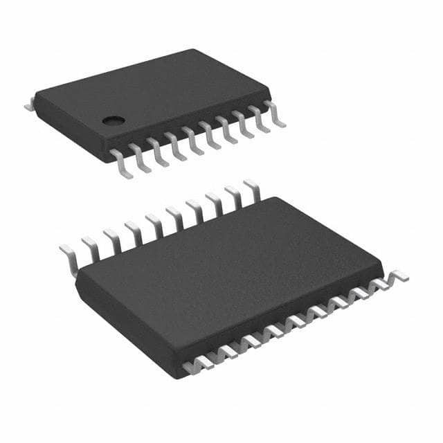
This device features a 2:4 fanout ratio and operates within a voltage range of 2.375V to 3.63V. The operating temperature range is -40°C to 85°C, making it suitable for demanding environments. It is packaged in a 20-TSSOP (0.173", 4.40mm Width) format and is designed for surface mount installation.
The NB3L8533DTG is ideal for applications requiring precise clock signal distribution and level translation. Its robust specifications and compact package make it a versatile component for modern electronic designs.
| Qty | Low | High |
|---|---|---|
| 1+ | $4.44 | $4.44 |
Estimated market price range - modelled values for guidance only, not live distributor offers.
The NB3L8533DTG operates within a voltage range of 2.375V to 3.63V.
The NB3L8533DTG is packaged in a 20-TSSOP surface mount package.
-40°C to 85°C.
It is marked as RoHS3 compliant, but compliance status is unverified.