

| Distributor | Stock | Pricing | MOQ | PKG | Lead Time | Date Code | On Order Quantity | On Order Delivery | |
|---|---|---|---|---|---|---|---|---|---|
|
2,500 pcs
|
2500 pcs | On Request | 1 | On Request | On Request | On Request | On Request | On Request | |
|
22 pcs
|
22 pcs | On Request | 1 | On Request | On Request | On Request | On Request | On Request | |
| On Request | On Request | 1 | On Request | On Request | On Request | On Request | On Request |
| Category | |
| Manufacturer Name | |
| Differential | |
| Frequency | |
| Input | |
| Mounting Type | |
| Number of Circuits | |
| Operating Temperature | |
| Output | |
| Ratio | |
| Storage Temperature | |
| Supplier Device Package | |
| Supplier Package | |
| Tape & Reel | |
| Type | |
| Voltage |
The On Semiconductor NB3L553MNR4G is an integrated circuit functioning as a fanout buffer, specifically designed for clock signal distribution. It supports input and output signals compatible with LVCMOS and LVTTL logic levels.
This buffer operates at frequencies up to 200 MHz, making it suitable for various timing applications. The device accepts a wide operating voltage range from 2.375V to 5.25V and can function within an ambient temperature range of -40°C to 85°C. It is configured with a 1:4 ratio, indicating it can drive four outputs from a single input.
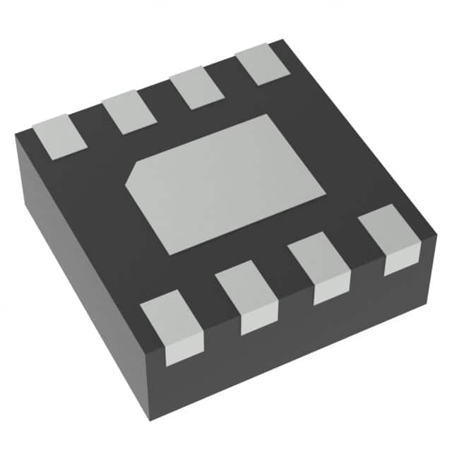
The NB3L553MNR4G is housed in an 8-pin DFN (Dual Flat No-lead) package, specifically an 8-VFDFN with an exposed pad, designed for surface mounting. This package type is chosen for its small footprint and good thermal performance, suitable for compact electronic designs.
| Qty | Low | High |
|---|---|---|
| 1+ | $4.44 | $4.44 |
Estimated market price range - modelled values for guidance only, not live distributor offers.
The operating voltage range is 2.375V to 5.25V.
The NB3L553MNR4G supports frequencies up to 200 MHz.
It is supplied in an 8-VFDFN Exposed Pad package.
The operating temperature range is -40°C to 85°C.
It supports LVCMOS and LVTTL logic levels for both input and output.