

| Distributor | Stock | Pricing | MOQ | PKG | Lead Time | Date Code | On Order Quantity | On Order Delivery | |
|---|---|---|---|---|---|---|---|---|---|
|
615 pcs
|
615 pcs | On Request | 1 | On Request | On Request | On Request | On Request | On Request |
| Category | |
| Manufacturer Name | |
| Differential | |
| Frequency | |
| Input | |
| Input Type | |
| Mounting Type | |
| Number of Circuits | |
| Number of Outputs | |
| Operating Temperature | |
| Output | |
| Output Type | |
| Ratio | |
| Supplier Device Package | |
| Type | |
| Voltage |
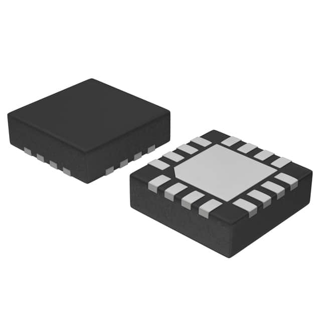
The NB3L202KMNG is an integrated circuit clock buffer manufactured by On Semiconductor. It provides a 1:2 output configuration suitable for distributing clock signals in electronic systems. The device supports input clock frequencies up to 350MHz and has two outputs with HCSL output type. It is designed for applications requiring precise clock distribution with minimal skew and jitter.
This clock buffer operates over a temperature range from -40°C to 85°C and is available in a 16-QFN package. Its typical propagation delay is 1 nanosecond, with output-to-output skew limited to 100 picoseconds. Rise and fall times are approximately 500 picoseconds, and maximum additive RMS phase jitter is 80 femtoseconds. The device supports multiple input types, including HCSL, LVDS, and LVPECL, making it versatile for various high-speed digital applications.
| Qty | Low | High |
|---|---|---|
| 1+ | $4.44 | $4.44 |
Estimated market price range - modelled values for guidance only, not live distributor offers.
The maximum input clock frequency supported is 350 MHz.
It operates with a supply voltage of 2.5 V ±5% to 3.3 V ±10%.
It has two outputs.
The output type is HCSL.
The typical propagation delay is 1 nanosecond.
The maximum output-to-output skew is 100 picoseconds.