

| Distributor | Stock | Pricing | MOQ | PKG | Lead Time | Date Code | On Order Quantity | On Order Delivery | |
|---|---|---|---|---|---|---|---|---|---|
|
45,696 pcs
|
45696 pcs | On Request | 1 | On Request | On Request | On Request | On Request | On Request |
| Category | |
| Manufacturer Name | |
| AEC Qualified | |
| Automotive Grade | |
| Differential | |
| Duty Cycle | |
| Frequency | |
| Industrial Grade | |
| Input | |
| Input Type | |
| Lead Spacing | |
| Medical Grade | |
| Military Grade | |
| Mounting Type | |
| Number of Circuits | |
| Operating Temperature | |
| Output | |
| Ratio | |
| Supplier Device Package | |
| Supplier Package | |
| Supply Current | |
| Tape & Reel | |
| Type | |
| Voltage |
The NB3H83905CDG from ON Semiconductor is a versatile 1:6 LVTTL/LVCMOS clock fanout buffer. It is designed to accept a crystal input from 3 MHz to 40 MHz or a single-ended LVCMOS clock up to 100 MHz.
This device supports flexible supply voltages, with a core VDD ranging from 1.8 V ± 0.2 V, 2.5 V ± 5%, or 3.3 V ± 5%. The outputs are powered by a separate VDDO supply, which can also be set to 1.8 V, 2.5 V, or 3.3 V, provided VDD is greater than or equal to VDDO. The buffer features synchronous output enable lines for glitch-free operation and is compatible with ICS83905 and PI6C10806.
Key electrical characteristics include a low output-to-output skew of 80 ps maximum and a phase noise floor of -160 dBc at 1 MHz. The NB3H83905CDG operates within an industrial temperature range of -40°C to 85°C.
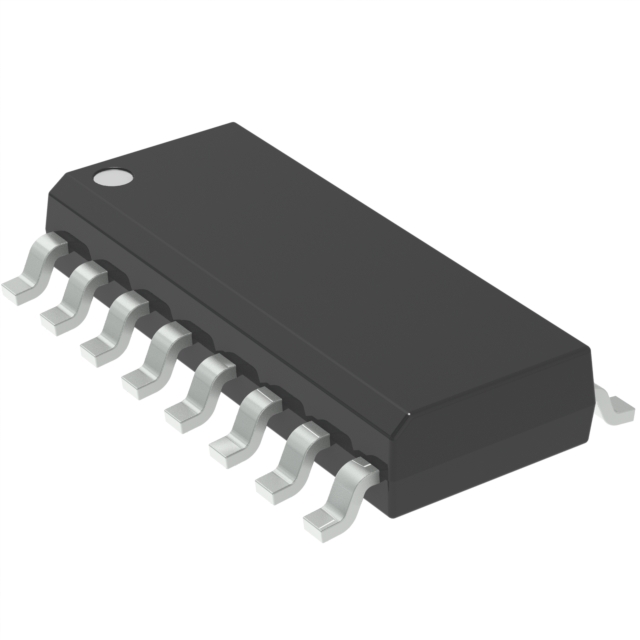
Packaged in a 16-SOIC surface mount package, this component is suitable for various clock distribution applications where reliable signal integrity and low skew are critical.
| Qty | Low | High |
|---|---|---|
| 1+ | $4.44 | $4.44 |
Estimated market price range - modelled values for guidance only, not live distributor offers.
The NB3H83905CDG accepts a clock input frequency of up to 100 MHz.
The device supports a core VDD and output VDDO range from 1.6V to 3.465V, with specific options for 1.8V, 2.5V, and 3.3V.
The NB3H83905CDG operates within an industrial temperature range of -40°C to 85°C.
This clock buffer is available in a 16-SOIC package.
The RoHS status is listed as RoHS3 Compliant.