

| Distributor | Stock | Pricing | MOQ | PKG | Lead Time | Date Code | On Order Quantity | On Order Delivery | |
|---|---|---|---|---|---|---|---|---|---|
|
7,798 pcs
|
7798 pcs | On Request | 1 | On Request | On Request | On Request | On Request | On Request |
| Category | |
| Manufacturer Name | |
| Differential | |
| Frequency | |
| Input | |
| Mounting Type | |
| Number of Circuits | |
| Operating Temperature | |
| Output | |
| Ratio | |
| Supplier Device Package | |
| Tape & Reel | |
| Type | |
| Voltage |
The NB3F8L3010CMNTWG is a 3:10 fanout buffer from ON Semiconductor, designed for clock signal distribution and multiplexing applications. This device supports input signals including HCSL, LVDS, LVPECL, SSTL, and Crystal, with LVCMOS and LVTTL outputs.
It operates within a voltage range of 2.375V to 3.465V and can handle frequencies up to 200 MHz. The buffer is specified for operation across a temperature range of -40°C to 85°C.
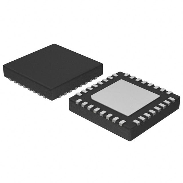
Packaged in a 32-VFQFN exposed pad, the NB3F8L3010CMNTWG is designed for surface mount applications. The compact 32-QFN (5x5) supplier package makes it suitable for space-constrained designs.
This component is RoHS3 compliant and has an MSL rating of 1 Unlimited.
| Qty | Low | High |
|---|---|---|
| 1+ | $4.44 | $4.44 |
Estimated market price range - modelled values for guidance only, not live distributor offers.
The operating voltage for the NB3F8L3010CMNTWG is between 2.375V and 3.465V.
The operating temperature range is -40°C to 85°C.
The maximum frequency supported is 200 MHz.
The NB3F8L3010CMNTWG is supplied in a 32-VFQFN Exposed Pad package.
This buffer has a fanout ratio of 3:10.