

| Distributor | Stock | Pricing | MOQ | PKG | Lead Time | Date Code | On Order Quantity | On Order Delivery | |
|---|---|---|---|---|---|---|---|---|---|
|
5,000 pcs
|
5000 pcs | On Request | 1 | On Request | On Request | On Request | On Request | On Request |
| Category | |
| Manufacturer Name | |
| Differential | |
| Divider | |
| Frequency | |
| Input | |
| Lead Style | |
| Mounting Type | |
| Number of Circuits | |
| Operating Temperature | |
| Output | |
| PLL | |
| Ratio | |
| Supplier Device Package | |
| Supplier Package | |
| Type | |
| Voltage |
The NB2309AI1HDTR2G is a zero delay buffer IC from ON Semiconductor, categorized under Clock Generators, PLLs, and Frequency Synthesizers. This component is designed for efficient clock signal distribution within electronic systems.
Key electrical specifications include an operating voltage range of 3V to 3.6V, with a typical operating voltage of 3.3V. It supports a maximum frequency of 133.33MHz and features a 1:9 ratio for clock output. The device is equipped with a PLL and bypass functionality, and it operates within a temperature range of -40°C to 85°C.
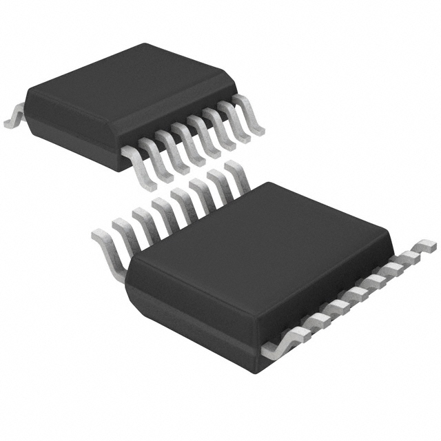
Packaged in a 16-TSSOP (0.173", 4.40mm Width) surface mount configuration, the NB2309AI1HDTR2G is suitable for applications requiring precise clock timing. It has a single circuit and is designed for clock input and output signals, with no differential signaling capabilities.
This buffer is RoHS3 compliant and has an MSL rating of 1 Unlimited, indicating its suitability for a wide range of manufacturing environments. Its REACH status is unaffected.
| Qty | Low | High |
|---|---|---|
| 1+ | $7.01 | $7.01 |
Estimated market price range - modelled values for guidance only, not live distributor offers.
The operating voltage for the NB2309AI1HDTR2G is between 3V and 3.6V.
The NB2309AI1HDTR2G operates within a temperature range of -40°C to 85°C.
The NB2309AI1HDTR2G is supplied in a 16-TSSOP (0.173", 4.40mm Width) package.
The NB2309AI1HDTR2G is RoHS3 Compliant.