

| Distributor | Stock | Pricing | MOQ | PKG | Lead Time | Date Code | On Order Quantity | On Order Delivery | |
|---|---|---|---|---|---|---|---|---|---|
|
143 pcs
|
143 pcs | On Request | 1 | On Request | On Request | OGHE | On Request | On Request |
| Category | |
| Manufacturer Name | |
| Differential | |
| Divider | |
| Frequency | |
| Input | |
| Mounting Type | |
| Number of Circuits | |
| Operating Temperature | |
| Operating Voltage | |
| Output | |
| PLL | |
| Ratio | |
| Supplier Device Package | |
| Type | |
| Voltage |
The NB2308AI2DTR2G from ON Semiconductor is a versatile 3.3V zero delay clock buffer. It is designed to efficiently distribute high-speed clocks within electronic systems. The device features an on-chip PLL that locks to an input clock signal, ensuring minimal propagation delay.
Key electrical specifications include an input frequency range of 15 MHz to 133 MHz and an output frequency of up to 133.3 MHz. The buffer offers low output-to-output skew, guaranteed to be less than 200 ps, and device-to-device skew less than 700 ps. It operates within a voltage range of 3V to 3.6V and has an operating temperature range of -40°C to 85°C.
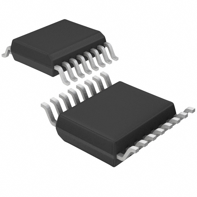
This clock buffer is available in a 16-TSSOP package, suitable for surface mount applications. It provides 8 outputs organized in two banks, which can be controlled by select inputs. The NB2308AI2DTR2G supports multiple configurations, allowing for frequency multiplication (2X, 4X) or division (REF/2) depending on the feedback path setup, making it adaptable for various system requirements.
| Qty | Low | High |
|---|---|---|
| 1+ | $7.01 | $7.01 |
Estimated market price range - modelled values for guidance only, not live distributor offers.
The NB2308AI2DTR2G operates at 3.3V, with a supported range from 3V to 3.6V.
The NB2308AI2DTR2G is available in a 16-TSSOP package.
The operating temperature range for the NB2308AI2DTR2G is -40°C to 85°C.
The NB2308AI2DTR2G is RoHS3 Compliant.
The maximum input frequency for the NB2308AI2DTR2G is 133 MHz.
The output-to-output skew is guaranteed to be less than 200 ps.