

| Distributor | Stock | Pricing | MOQ | PKG | Lead Time | Date Code | On Order Quantity | On Order Delivery | |
|---|---|---|---|---|---|---|---|---|---|
|
4,000 pcs
|
4000 pcs | On Request | 1 | On Request | On Request | On Request | On Request | On Request |
| Category | |
| Manufacturer Name | |
| Channel Type | |
| Channels per Circuit | |
| Data Rate | |
| Halogen Free | |
| Input Signal | |
| Mounting Type | |
| Number of Circuits | |
| Operating Temperature | |
| Operating Voltage | |
| Output Signal | |
| Output Type | |
| Propagation Delay | |
| Supplier Device Package | |
| Supplier Package | |
| Translator Type |
The NB100LVEP91DWR2G is a versatile translator IC from On Semiconductor designed for level translation between various logic families and differential LVNECL outputs. It supports input signals including LVPECL, LVTTL, LVCMOS, HSTL, CML, and LVDS, translating them to differential LVNECL output signals operating at -2.5 V or -3.3 V.
Key electrical specifications include a maximum input clock frequency exceeding 2.0 GHz and a maximum input data rate over 2.0 Gb/s. The device exhibits a typical propagation delay of 500 ps. It operates across a voltage range of 2.375 V to 3.8 V for VCC and -2.375 V to -3.8 V for VEE, with GND at 0 V.
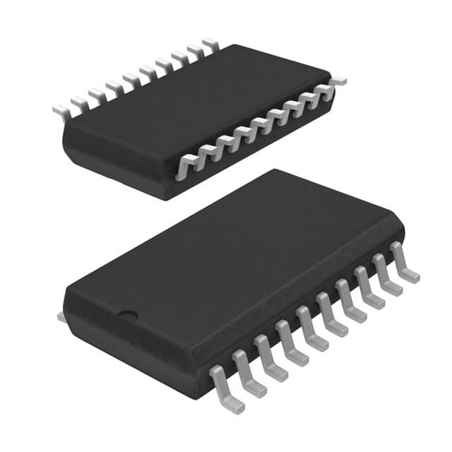
This translator is housed in a 20-SOIC package with surface mount mounting type. The Q outputs default to a low state when inputs are open or at GND, ensuring stability. The device is Pb-Free, Halogen Free, and RoHS compliant.
Applications for this translator include signal integrity management in high-speed digital systems, interfacing between different logic levels in complex circuit designs, and clock distribution networks requiring precise level shifting.
| Qty | Low | High |
|---|---|---|
| 1+ | $0.12 | $0.12 |
Estimated market price range - modelled values for guidance only, not live distributor offers.
The maximum input clock frequency is greater than 2.0 GHz.
The typical propagation delay is 500 ps.
The operating voltage ranges are VCC from 2.375 V to 3.8 V, VEE from -2.375 V to -3.8 V, and GND at 0 V.
The operating temperature range is -40°C to 85°C (TA).
The NB100LVEP91DWR2G is available in a 20-SOIC package with a width of 0.295 inches (7.50mm).
It supports CML, HSTL, LVCMOS, LVDS, LVPECL, and LVTTL input signals.
It provides differential LVNECL output signals.