

| Distributor | Stock | Pricing | MOQ | PKG | Lead Time | Date Code | On Order Quantity | On Order Delivery | |
|---|---|---|---|---|---|---|---|---|---|
|
276 pcs
|
276 pcs | On Request | 1 | On Request | On Request | On Request | On Request | On Request |
| Category | |
| Manufacturer Name | |
| Circuit | |
| Independent Circuits | |
| Mounting Type | |
| Operating Temperature | |
| Propagation Delay | |
| Supplier Device Package | |
| Supplier Package | |
| Type | |
| Voltage | |
| Voltage Supply Source |
The NB100LVEP56MNG is a dual, fully differential 2:1 multiplexer designed by ON Semiconductor. Its differential data path makes it suitable for multiplexing low skew clock or differential data signals. The device supports both individual and common select inputs, compatible with LVECL and LVCMOS voltage levels.
Key electrical characteristics include a maximum input clock frequency exceeding 2.5 GHz and a maximum input data rate over 2.5 Gb/s. Typical propagation delays are 525 ps. The device operates in PECL mode with VCC from 2.375 V to 3.8 V (VEE = 0 V) or in NECL mode with VEE from -2.375 V to -3.8 V (VCC = 0 V).
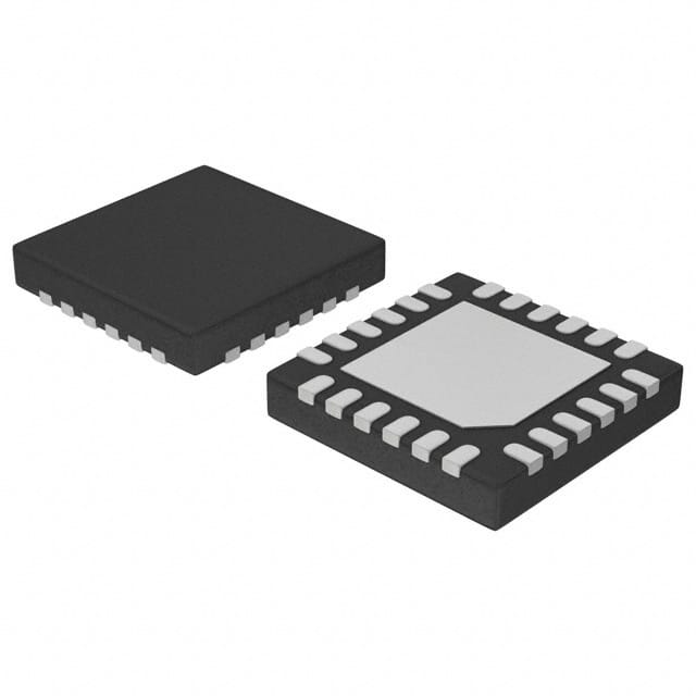
This multiplexer is housed in a low-profile 24-QFN package with surface mount mounting type. It is designed for applications requiring high-speed differential signal routing and multiplexing.
| Qty | Low | High |
|---|---|---|
| 1+ | $1.27 | $1.27 |
Estimated market price range - modelled values for guidance only, not live distributor offers.
The operating voltage range for the NB100LVEP56MNG in PECL Mode is 2.375 V to 3.8 V.
The operating voltage range for the NB100LVEP56MNG in NECL Mode is -3.8 V to -2.375 V.
The package type for the NB100LVEP56MNG is 24-VFQFN Exposed Pad.
The operating temperature range for the NB100LVEP56MNG is -40°C to 85°C.
The maximum input clock frequency of the NB100LVEP56MNG is > 2.5 GHz.
The typical propagation delay of the NB100LVEP56MNG is 525 ps.
The NB100LVEP56MNG has a 2 x 2:1 circuit.