

| Distributor | Stock | Pricing | MOQ | PKG | Lead Time | Date Code | On Order Quantity | On Order Delivery | |
|---|---|---|---|---|---|---|---|---|---|
|
2,753 pcs
|
2753 pcs | On Request | 1 | On Request | On Request | On Request | On Request | On Request |
| Category | |
| Manufacturer Name | |
| Access Time | |
| Clock Frequency | |
| Lead Style | |
| Memory Format | |
| Memory Interface | |
| Memory Organization | |
| Memory Size | |
| Memory Type | |
| Mounting Type | |
| Operating Temperature | |
| Operating Voltage | |
| Package / Case | |
| Supplier Device Package | |
| Technology | |
| Voltage | |
| Write Cycle Time |
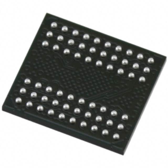
This Micron Technology MT46H32M16LFBF-5 IT:C is a 512Mbit DRAM memory IC. It utilizes LPDDR SDRAM technology and features a parallel memory interface. The component operates with a supply voltage range of 1.70V to 1.95V and supports clock frequencies up to 200 MHz, with an access time of 5.0 ns.
The memory is organized as 32M x 16 and is housed in a 60-VFBGA (8x9mm) package, suitable for surface mounting. The operating temperature range is -40°C to 85°C (TA).
Key features include bidirectional data strobe, internal pipelined DDR architecture, differential clock inputs, and 4 internal banks for concurrent operation. It also supports programmable burst lengths, auto refresh, self refresh modes, and temperature-compensated self refresh.
This component is designed for applications requiring high-speed data access and storage within a compact form factor. Its specifications make it suitable for various electronic systems where memory performance and density are critical.
| Qty | Low | High |
|---|---|---|
| 1+ | $1.28 | $1.28 |
Estimated market price range - modelled values for guidance only, not live distributor offers.
The device supports a core and I/O voltage of 1.8V/1.8V, with a supply voltage range of 1.70V to 1.95V.
It comes in a 60-ball VFBGA package measuring 8mm x 9mm.
The device is rated for -40°C to +85°C (ambient) and an automotive grade of -40°C to +105°C.
It has 512Mbit capacity organized as 32M x 16 (8 Meg x 16 x 4 banks).
It supports 200 MHz and 166 MHz clock frequencies.
The access time is 5.0 ns.
The write cycle time is 15 ns.