

| Distributor | Stock | Pricing | MOQ | PKG | Lead Time | Date Code | On Order Quantity | On Order Delivery | |
|---|---|---|---|---|---|---|---|---|---|
|
1,388 pcs
|
1388 pcs | On Request | 1 | On Request | On Request | On Request | On Request | On Request |
| Category | |
| Manufacturer Name | |
| Current | |
| Frequency | |
| Gain | |
| Lead Spacing | |
| Mounting Type | |
| Power | |
| Supplier Device Package | |
| Supplier Package | |
| Tape & Reel | |
| Technology | |
| VSWR | |
| Voltage |
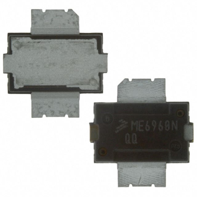
The MRFE6S9060NR1 from NXP Semiconductors is a high-performance RF Power Field Effect Transistor. It is an N-Channel, enhancement-mode, lateral MOSFET designed for broadband applications with frequencies up to 1000 MHz. This device offers high gain and broadband performance, making it suitable for large-signal, common-source amplifier applications in 28 volt base station equipment.
Key electrical characteristics include a typical power gain of 21.1 dB at 880 MHz under IS-95 CDMA conditions, with a drain efficiency of 33% and an ACPR of -45.7 dBc. For GSM EDGE applications, it provides a typical power gain of 20 dB and a drain efficiency of 46%. In standard GSM applications, it achieves a power gain of 20 dB and a drain efficiency of 63%.
The MRFE6S9060NR1 is characterized with series equivalent large-signal impedance parameters and features integrated ESD protection. It is housed in a 225°C capable plastic package, specifically the TO-270-2 (TO-270AA) style. The mounting type is surface mount, and it is supplied in tape and reel packaging.
| Qty | Low | High |
|---|---|---|
| 1+ | $0.99 | $0.99 |
Estimated market price range - modelled values for guidance only, not live distributor offers.
The maximum operation voltage is 32 Vdc.
The MRFE6S9060NR1 is supplied in a TO-270-2 package.
The operating junction temperature is 225 °C.
The MRFE6S9060NR1 is RoHS3 Compliant.