

| Distributor | Stock | Pricing | MOQ | PKG | Lead Time | Date Code | On Order Quantity | On Order Delivery | |
|---|---|---|---|---|---|---|---|---|---|
|
325 pcs
|
325 pcs | On Request | 1 | On Request | On Request | On Request | On Request | On Request |
| Category | |
| Manufacturer Name | |
| AEC Qualified | |
| Automotive Grade | |
| Current | |
| Frequency | |
| Gain | |
| Industrial Grade | |
| Medical Grade | |
| Military Grade | |
| Mounting Type | |
| Power | |
| Storage Temperature | |
| Supplier Device Package | |
| Tape & Reel | |
| Technology | |
| VSWR | |
| Voltage |
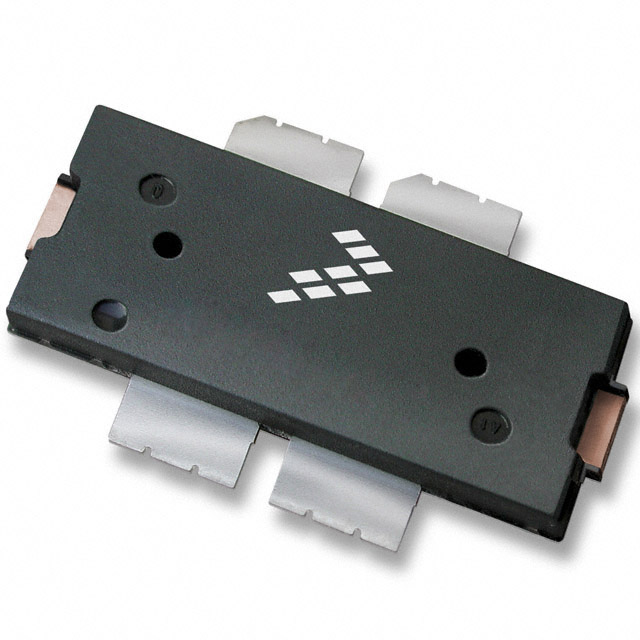
The NXP Semiconductors MRF6S19100NR1 is a lateral N-channel enhancement-mode LDMOS RF power MOSFET. It is designed for CDMA base station applications, operating within the 1930 to 1990 MHz frequency range. This device is suitable for TDMA, CDMA, and multicarrier amplifier applications, particularly in Class AB for PCN/PCS/cellular radio and WLL applications.
Key electrical specifications include a drain-source voltage of up to 68V, a gate-source voltage of up to 12V, and a quiescent current of 950 mA. It offers a typical power gain of 14.5 dB and an average output power of 22 Watts at 1987.5 MHz under 2-carrier N-CDMA conditions. The device is capable of handling a 5:1 VSWR at 28 Vdc and 100 Watts CW.
Packaged in a TO-270AB surface-mount package, the MRF6S19100NR1 features integrated ESD protection and is internally matched for ease of use. It is qualified for operation up to 32 VDD. The RoHS status is listed as RoHS3 Compliant, and the Moisture Sensitivity Level (MSL) is 1.
| Qty | Low | High |
|---|---|---|
| 1+ | $0.99 | $0.99 |
Estimated market price range - modelled values for guidance only, not live distributor offers.
The MRF6S19100NR1 is qualified up to a maximum of 32 VDD operation.
The MRF6S19100NR1 is supplied in a TO-270AB package.
The RoHS status is RoHS3 Compliant.
The Moisture Sensitivity Level (MSL) is 1.
The typical power gain is 14.5 dB.
The typical average output power is 22 Watts.
The operating frequency range is 1930 to 1990 MHz.