

| Distributor | Stock | Pricing | MOQ | PKG | Lead Time | Date Code | On Order Quantity | On Order Delivery | |
|---|---|---|---|---|---|---|---|---|---|
|
3,500 pcs
|
3500 pcs | On Request | 1 | On Request | On Request | On Request | On Request | On Request |
| Category | |
| Manufacturer Name | |
| Current | |
| Frequency | |
| Gain | |
| Mounting Type | |
| Operating Voltage | |
| Power | |
| Supplier Device Package | |
| Tape & Reel | |
| Technology | |
| VSWR | |
| Voltage |
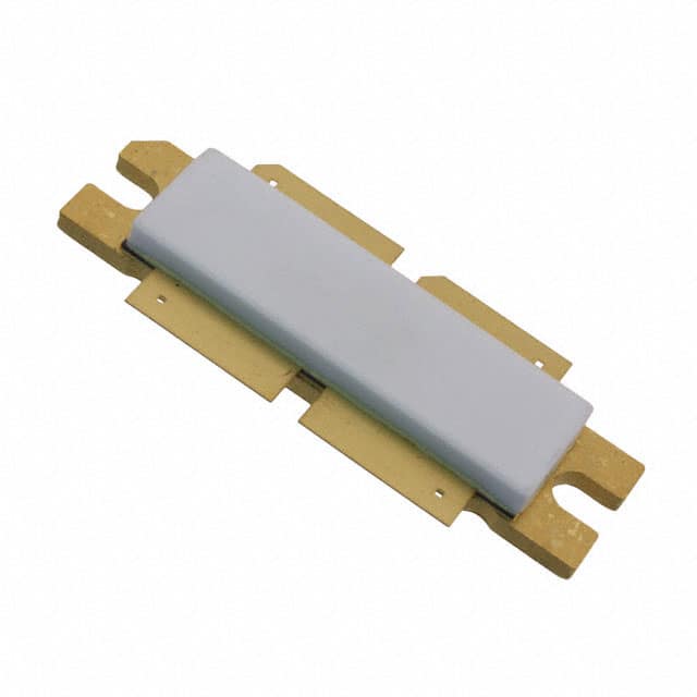
The MRF6P21190HR6 by NXP Semiconductors is a lateral N-channel enhancement-mode MOSFET designed for RF power applications, specifically W-CDMA base stations operating from 2110 to 2170 MHz. It is suitable for TDMA, CDMA, and multicarrier amplifier applications, intended for use in Class AB amplifiers for PCN/PCS/cellular radio and WLL.
Key electrical characteristics include a typical power gain of 15.5 dB and a drain efficiency of 26.5% under specific W-CDMA test conditions (VDD = 28V, IDQ = 1900 mA, Pout = 44 Watts Avg.). It can handle up to 190 Watts CW output power at 28 Vdc and 2140 MHz with a 10:1 VSWR.
The device features internally matched circuitry for ease of use and integrated ESD protection. It is qualified for operation up to a maximum of 32 VDD. The component is supplied in tape and reel packaging, indicated by the R6 suffix, with 150 units per 56 mm tape width on a 13-inch reel. Mounting is via chassis mount.
Maximum ratings include a Drain-Source Voltage (VDSS) of +68 Vdc and a Gate-Source Voltage (VGS) of +12 Vdc. The operating junction temperature can reach up to 225 °C.
| Qty | Low | High |
|---|---|---|
| 1+ | $0.99 | $0.99 |
Estimated market price range - modelled values for guidance only, not live distributor offers.
The typical average output power is 44 Watts.
The typical power gain is 15.5 dB.
The device is designed for frequencies from 2110 to 2170 MHz.
The maximum operating junction temperature is 225 °C.
This component is chassis mounted.
The Moisture Sensitivity Level is 1.