
MMBF4393LT1
On Semiconductor
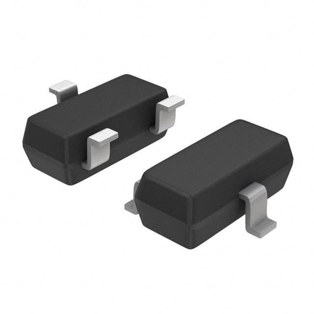
The MMBF4393LT1 is an N-Channel JFET transistor from On Semiconductor in a SOT-23 package. It offers a Drain-Source Voltage of 30V.


| Distributor | Stock | Pricing | MOQ | PKG | Lead Time | Date Code | On Order Quantity | On Order Delivery | |
|---|---|---|---|---|---|---|---|---|---|
|
2,800 pcs
|
2800 pcs | On Request | 1 | On Request | On Request | On Request | On Request | On Request |
| Category | |
| Manufacturer Name | |
| Halogen Free | |
| Input Capacitance | |
| Mounting Type | |
| Tape & Reel | |
| Thermal Resistance |
The MMBF4392LT1 is an N-Channel JFET switching transistor manufactured by On Semiconductor. It is designed for various switching applications and comes in a compact SOT-23 surface-mount package.
Key electrical characteristics include a maximum drain-source voltage of 30V and a maximum forward gate current of 50mAdc. The device exhibits a typical zero-gate-voltage drain current (IDSS) ranging from 25mA to 75mA at 15V drain-source voltage. Its gate-source cutoff voltage (VGS(off)) is typically -2.0Vdc, with a maximum of -5.0Vdc. The static drain-source on-resistance (rDS(on)) is a maximum of 60 Ohm at 1.0mAdc drain current.
Thermal performance is supported by a total device dissipation of 225mW at 25°C on an FR-5 board, with a junction-to-ambient thermal resistance of 556°C/W. The operating and storage temperature range is from -55°C to +150°C.
This JFET is Pb-free and Halogen-free, complying with RoHS standards. Its SOT-23 package makes it suitable for space-constrained designs requiring surface mounting.
| Qty | Low | High |
|---|---|---|
| 1+ | $0.99 | $0.99 |
Estimated market price range - modelled values for guidance only, not live distributor offers.
The maximum drain-source voltage (VDS) for the MMBF4392LT1 is 30 Vdc.
The zero-gate-voltage drain current (IDSS) for the MMBF4392LT1 ranges from a minimum of 25mA to a maximum of 75mA at 15V VDS.
The maximum gate-source cutoff voltage (VGS(off)) for the MMBF4392LT1 is -5V.
The MMBF4392LT1 is available in a SOT-23 surface-mount package.
The operating temperature range for the MMBF4392LT1 is -55°C to +150°C.