

| Distributor | Stock | Pricing | MOQ | PKG | Lead Time | Date Code | On Order Quantity | On Order Delivery | |
|---|---|---|---|---|---|---|---|---|---|
|
30,850 pcs
|
30850 pcs | On Request | 1 | On Request | On Request | 2020+ | On Request | On Request |
| Category | |
| Manufacturer Name | |
| Applications | |
| Logic Voltage | |
| Mounting Type | |
| Operating Temperature | |
| Output Voltage | |
| Package / Case | |
| Supplier Device Package | |
| Voltage |
The MD1730-V/M2 from Microchip Technology is an 8-channel ultrasound Continuous Waveform (CW) transmitter featuring an integrated beamformer. Designed for high-performance CW Doppler modes in medical ultrasound imaging systems, it minimizes phase noise with a dedicated signal path.
Key electrical specifications include an output voltage swing of ±1V to ±6Vp-p, ultra-low phase noise of -160 dbc/Hz at 1 kHz offset and 5 MHz, and an 8-bit programmable phase delay per channel. The device supports an input clock frequency up to 250 MHz and features a fast SPI interface operating up to 200 MHz, compatible with daisy chaining and broadcasting modes. Control I/O pins operate with LVCMOS 2.5V logic.
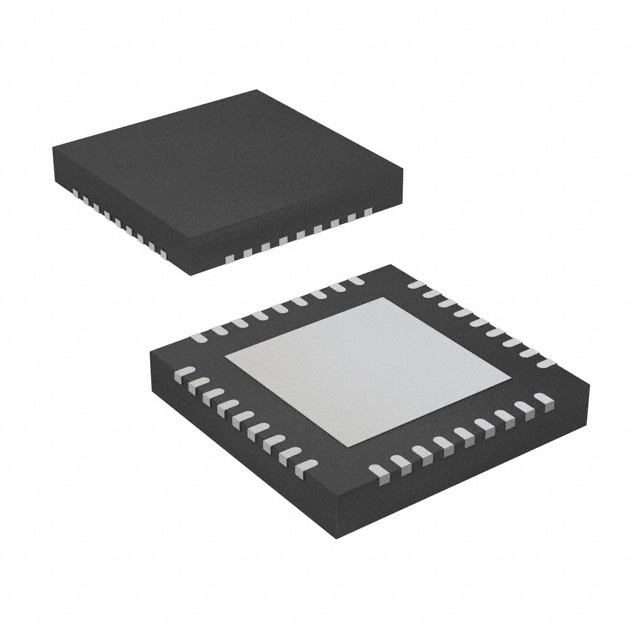
This IC is suitable for applications such as medical ultrasound imaging systems for cardiovascular applications, ultrasound fetal heart monitoring devices, and ultrasound flow meters. It is available in a 36-lead VQFN package with an exposed thermal pad, designed for surface mounting.
The MD1730-V/M2 enables programmable CW frequencies from a single clock source through its internal frequency divider. For example, with a 160 MHz input clock and a divider set to 16, an output CW frequency of 5 MHz can be achieved with a phase delay step size of 6.25 ns.
| Qty | Low | High |
|---|---|---|
| 1+ | $0.75 | $0.75 |
Estimated market price range - modelled values for guidance only, not live distributor offers.
The CW output range is ±1V to ±6Vp-p.
It offers ultra-low phase noise of -160 dbc/Hz at 1 kHz offset and 5 MHz.
The beamforming phase delay is programmable with 8-bit resolution per channel.
The input clock frequency can be up to 250 MHz.
The control I/O pins use LVCMOS 2.5V logic.
The operating temperature range is 0°C to 85°C.
It is supplied in a 36-VFQFN Exposed Pad package.