

| Distributor | Stock | Pricing | MOQ | PKG | Lead Time | Date Code | On Order Quantity | On Order Delivery | |
|---|---|---|---|---|---|---|---|---|---|
|
3,500 pcs
|
3500 pcs | On Request | 1 | On Request | On Request | On Request | On Request | On Request |
| Category | |
| Manufacturer Name | |
| Differential | |
| Frequency | |
| Input | |
| Lead Spacing | |
| Main Purpose | |
| Mounting Type | |
| Number of Circuits | |
| Operating Temperature | |
| Output | |
| PLL | |
| Ratio | |
| Supplier Device Package | |
| Voltage | |
| Voltage Supply |
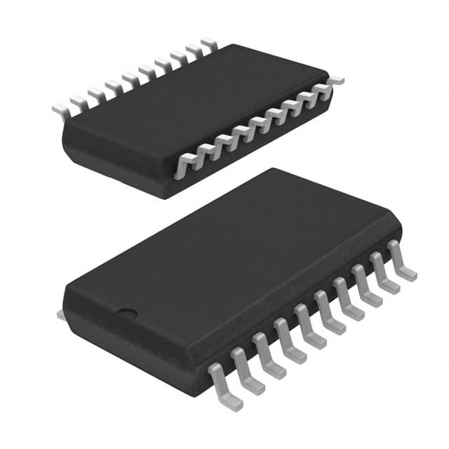
The MC88916DW80 from NXP Semiconductors is an application-specific clock buffer designed for CISC/RISC microprocessor applications. This integrated circuit operates at a maximum frequency of 80MHz and features a 1:6 ratio for input to output signals.
It supports TTL input and CMOS, TTL output signal types, with a supply voltage range of 4.5V to 5.5V. The device operates within a temperature range of -40°C to 85°C. The MC88916DW80 is housed in a 20-SOIC surface mount package.
This clock buffer is suitable for designs requiring precise clock signal distribution and management within microprocessor systems. Its specifications make it a component for various embedded systems and digital logic applications.
| Qty | Low | High |
|---|---|---|
| 1+ | $3.70 | $3.70 |
Estimated market price range - modelled values for guidance only, not live distributor offers.
The maximum operating frequency of the MC88916DW80 is 80MHz.
The MC88916DW80 operates with a supply voltage range of 4.5V to 5.5V.
The MC88916DW80 has TTL input and CMOS, TTL output signal types.
The operating temperature range for the MC88916DW80 is -40°C to 85°C.
The MC88916DW80 is supplied in a 20-SOIC package.
Yes, the MC88916DW80 has an integrated PLL.