

| Distributor | Stock | Pricing | MOQ | PKG | Lead Time | Date Code | On Order Quantity | On Order Delivery | |
|---|---|---|---|---|---|---|---|---|---|
|
157,056 pcs
|
157056 pcs | On Request | 1 | On Request | On Request | On Request | On Request | On Request |
| Category | |
| Manufacturer Name | |
| Clock Frequency | |
| Current | |
| Function | |
| Halogen Free | |
| Input Capacitance | |
| Lead Style | |
| Max Propagation Delay @ V, Max CL | |
| Mounting Type | |
| Number of Bits per Element | |
| Number of Elements | |
| Operating Temperature | |
| Output Type | |
| SVHC Present | |
| Supplier Device Package | |
| Supplier Package | |
| Trigger Type | |
| Type | |
| Voltage |
The MC74VHC74DTG from On Semiconductor is a high-speed CMOS dual D-type flip-flop. Fabricated with silicon gate CMOS technology, it achieves high speed operation while maintaining low power dissipation. The device transfers the signal level applied to the D input to the Q output during the positive-going transition of the clock pulse. Independent Set (SD) and Reset (RD) inputs are provided, which are accomplished by setting the appropriate input low. The inputs are compatible with standard CMOS levels, and the device can be used as a level converter for interfacing 3.3V to 5.0V systems due to its full 5.0V CMOS level output swings. The internal circuits include a buffer output for high noise immunity and stable output. The input structures tolerate voltages up to 5.5V, allowing interface of 5V systems to 3V systems.
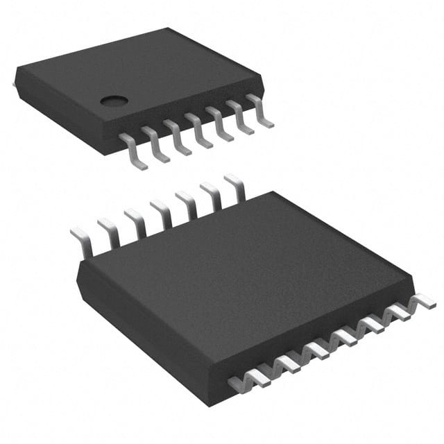
This flip-flop is designed for a 2.0V to 5.5V operating range and offers a high clock frequency of 115 MHz. It has a maximum propagation delay of 9.3ns at 5V and 50pF. The device features low power dissipation with a quiescent current of 2 µA. ESD performance is rated at greater than 2000V for the Human Body Model, and latchup performance exceeds 100 mA. The MC74VHC74DTG is supplied in a 14-TSSOP surface mount package with dimensions of 0.173 inches (4.40mm) width.
Key electrical characteristics include a maximum propagation delay of 9.3ns at 5V/50pF and an input capacitance of 4 pF. The device offers complementary output types and operates across a wide temperature range of -55°C to 125°C (TA). Its high noise immunity is indicated by VNIH = VNIL = 28% VCC. Power down protection is provided on inputs, and the device is pin and function compatible with other standard logic families.
| Qty | Low | High |
|---|---|---|
| 1+ | $0.86 | $0.86 |
Estimated market price range - modelled values for guidance only, not live distributor offers.
The operating voltage range is 2 V to 5.5 V.
The operating temperature range is -55°C to 125°C.
It comes in a 14-TSSOP package (0.173", 4.40mm width) for surface mount.
The maximum clock frequency is 115 MHz.
The maximum propagation delay is 9.3 ns at 5V and 50pF load.
The input capacitance is 4 pF.
The quiescent current is 2 µA.