

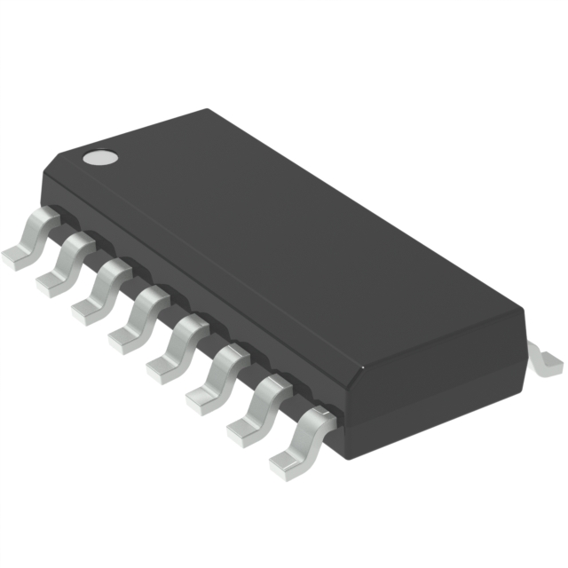
MC74LVX259DR2G The On Semiconductor MC74LVX259DR2G is an 8-bit addressable latch and 1-of-8 decoder. It operates within a voltage range of 2V to 3.6V and features a typical delay time of 7.0 ns.
Mfr Part #:

MC74LVX259DR2G

Available from 1 distributors
Mfr Name: On Semiconductor
On Semiconductor
The On Semiconductor MC74LVX259DR2G is an 8-bit addressable latch and 1-of-8 decoder. It operates within a voltage range of 2V to 3.6V and features a typical delay time of 7.0 ns.
✓ Total Stock: 40,000 pcs
$ Price Range: $1.22

MC74LVX259DR2G Available from 1 distributor

✓ Authorised
✓ Non-Authorised
Distributor Stock Pricing MOQ PKG Lead Time Date Code On Order Quantity On Order Delivery
Non-Authorised Inventory information
40,000 pcs
40000 pcs On Request 1 On Request On Request On Request On Request On Request

MC74LVX259DR2G Specifications Quick View

Most important parameters for selection – full specs in datasheet.
Category
Manufacturer Name
Circuit
Current
Delay Time
Independent Circuits
Logic Type
Mounting Type
Operating Temperature
Output Type
Supplier Device Package
Voltage

MC74LVX259DR2G Description

Short technical summary and product information.

The MC74LVX259DR2G from On Semiconductor is an 8-bit addressable latch fabricated with silicon gate CMOS technology. This device functions as both an addressable latch and a 1-of-8 decoder, suitable for general-purpose storage applications in digital systems.


Key electrical characteristics include an operating voltage range of 2V to 3.6V and a typical propagation delay of 7.0 ns at 3.3V. It offers high noise immunity with VNIH and VNIL at 28% VCC and CMOS-compatible outputs. The device also features power-down protection on inputs and outputs, balanced propagation delays, and Latchup performance exceeding 300 mA.


This latch is available in a 16-SOIC surface mount package. It operates within a temperature range of -40°C to 85°C. The MC74LVX259 is pin and function compatible with other standard logic families, making it a versatile component for interfacing 5.0V circuits to 3.0V circuits.

MC74LVX259DR2G Quick Information

Product Type: Latch
Canonical Name: 8-Bit Addressable Latch / 1-of-8 Decoder
Subcategory: Latches

MC74LVX259DR2G Compliance

RoHS Status: RoHS Compliant
Moisture Sensitivity Level (MSL): 1 Unlimited
REACH Status: REACH Unaffected

MC74LVX259DR2G Estimated Pricing

Qty Low High
1+ $1.22 $1.22

Estimated market price range - modelled values for guidance only, not live distributor offers.

MC74LVX259DR2G Features

  • 8-bit addressable latch and 1-of-8 decoder.
  • Operates from 2V to 3.6V supply voltage.
  • High speed with 7.0 ns typical delay.
  • 16-SOIC surface mount package.
  • Wide operating temperature range.

MC74LVX259DR2G Applications

  • Used as an addressable latch for data storage.
  • Serves as a 1-of-8 decoder or demultiplexer.
  • Memory mode retains previous latch states.
  • Reset mode forces all outputs low.
  • Ideal for level shifting between 5V and 3V circuits.

MC74LVX259DR2G FAQs

7 frequently asked questions generated from this part’s specifications.
What is the operating voltage range for the MC74LVX259DR2G?

The MC74LVX259DR2G operates within a voltage range of 2V to 3.6V.

What is the package type of the MC74LVX259DR2G?

The MC74LVX259DR2G is supplied in a 16-SOIC (0.154", 3.90mm Width) package.

What is the operating temperature range of the MC74LVX259DR2G?

The MC74LVX259DR2G can operate in a temperature range from -40°C to 85°C.

What is the typical delay time of this latch?

The typical delay time for this device is 7.0 ns.

What is the noise immunity of the MC74LVX259DR2G?

The device has a high noise immunity of 28% VCC.

What is the circuit configuration of the MC74LVX259DR2G?

The circuit configuration is 1:8.

What is the logic type of this component?

The logic type is D-Type, Addressable.

Home
Account

Categories