

| Distributor | Stock | Pricing | MOQ | PKG | Lead Time | Date Code | On Order Quantity | On Order Delivery | |
|---|---|---|---|---|---|---|---|---|---|
|
2,230 pcs
|
2230 pcs | On Request | 1 | On Request | On Request | On Request | On Request | On Request | |
|
2,188 pcs
|
2188 pcs | On Request | 1 | On Request | On Request | On Request | On Request | On Request |
| Category | |
| Manufacturer Name | |
| Current | |
| Input Logic Level | |
| Input Voltage | |
| Junction Temperature | |
| Latch-up Performance | |
| Lead Spacing | |
| Lead Style | |
| Logic Type | |
| Max Propagation Delay @ V, Max CL | |
| Mounting Type | |
| Number of Circuits | |
| Number of Inputs | |
| Operating Temperature | |
| Output Voltage | |
| SVHC Present | |
| Storage Temperature | |
| Supplier Device Package | |
| Supplier Package | |
| Supply Current | |
| Voltage |
The MC74ACT04DR2 from On Semiconductor is a hex inverter integrated circuit designed for high-performance applications. This device features six independent inverter gates, each with a single input and output.
Key electrical characteristics include an operating supply voltage range of 4.5V to 5.5V, with a typical maximum propagation delay of 8.5ns at 5V and 50pF load. The outputs can source and sink up to 24mA of current. The input logic level is specified at 2V.
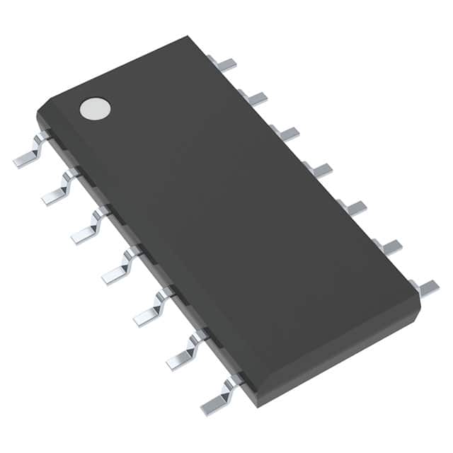
This component is housed in a 14-lead SOIC surface-mount package, measuring 0.154 inches (3.90mm) in width. It is designed for operation within an ambient temperature range of -40°C to 85°C.
The MC74ACT04DR2 is suitable for various digital logic applications requiring signal inversion.
| Qty | Low | High |
|---|---|---|
| 1+ | $0.22 | $0.22 |
Estimated market price range - modelled values for guidance only, not live distributor offers.
The operating supply voltage is 4.5V to 5.5V.
The device is available in a 14-SOIC (0.154", 3.90mm width) surface-mount package.
The operating temperature range is -40°C to +85°C.
It contains six inverter circuits, each with one input.
The maximum propagation delay is 8.5ns at 5V and 50pF load.
The output can source and sink ±24mA.
ESD withstand voltage is greater than 2000V human body model and greater than 1000V charged device model.