

| Distributor | Stock | Pricing | MOQ | PKG | Lead Time | Date Code | On Order Quantity | On Order Delivery | |
|---|---|---|---|---|---|---|---|---|---|
|
5,000 pcs
|
5000 pcs | On Request | 1 | On Request | On Request | On Request | On Request | On Request |
| Category | |
| Manufacturer Name | |
| Applications | |
| Interface | |
| Lead Spacing | |
| Mounting Type | |
| Supplier Device Package | |
| Supplier Package | |
| Voltage |
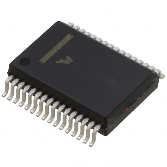
The NXP Semiconductors MC33993DWB is a specialized interface integrated circuit designed to detect the closing and opening of up to 22 switch contacts. It transfers switch status to a microprocessor unit (MCU) via a serial peripheral interface (SPI).
This device operates within a voltage range of 5.5 V to 26 V. It supports a switch input voltage range from -14 V to VPWR (40 V max) and interfaces directly with microprocessors using 3.3 V / 5.0 V SPI protocol. The MC33993DWB offers selectable wake-up on change of state and selectable wetting current options of 16 mA or 2.0 mA.
It features 8 programmable inputs (switches to battery or ground) and 14 switch-to-ground inputs. The device has low quiescent current, with typical VPWR standby current of 100 μA and VDD standby current of 20 μA, making it suitable for automotive and industrial products requiring low sleep state currents. An active interrupt (INT) is provided on change-of-switch state.
The MC33993DWB is packaged in a 32-pin wide-body SOIC (SOICW), reducing circuit board area. It is designed for surface mount applications.
| Qty | Low | High |
|---|---|---|
| 1+ | $6.39 | $6.39 |
Estimated market price range - modelled values for guidance only, not live distributor offers.
The operating voltage range is 5.5 V to 26 V.
The MC33993DWB uses an SPI serial interface.
The MC33993DWB is designed for automotive applications.
The switch input voltage range is -14 V to 40 V.
The typical standby current for VPWR is 100 μA.
The typical standby current for VDD is 20 μA.
The selectable wetting current options are 16 mA or 2.0 mA.