

| Distributor | Stock | Pricing | MOQ | PKG | Lead Time | Date Code | On Order Quantity | On Order Delivery | |
|---|---|---|---|---|---|---|---|---|---|
|
5,000 pcs
|
5000 pcs | On Request | 1 | On Request | On Request | On Request | On Request | On Request |
| Category | |
| Manufacturer Name | |
| Applications | |
| Interface | |
| Lead Spacing | |
| Mounting Type | |
| Operating Temperature | |
| Package / Case | |
| Supplier Device Package | |
| Voltage |
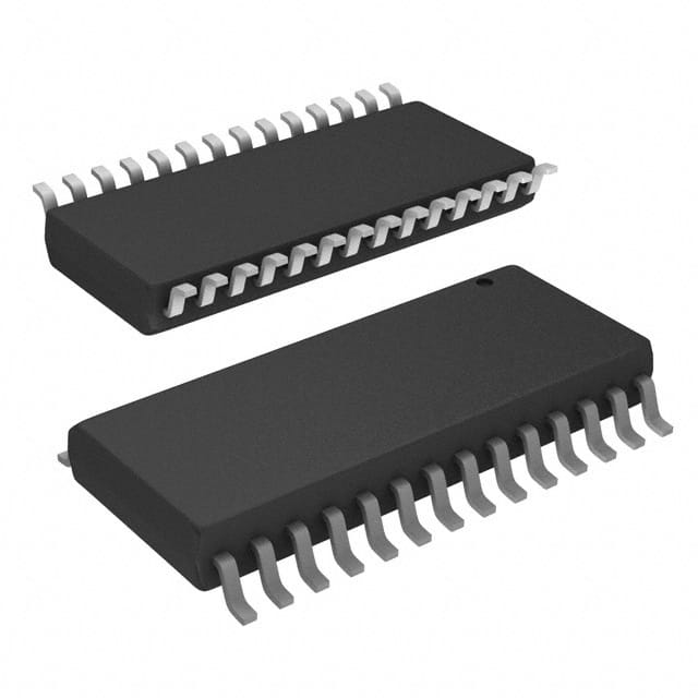
The NXP Semiconductors MC33989DW is a System Basis Chip designed for automotive Engine Control Units (ECUs). It integrates multiple functions, including a high-speed CAN physical interface capable of 1.0 MBaud communication.
This device features a supply voltage range of 5.5V to 18V and is housed in a 28-SOIC package suitable for surface mounting. Key electrical characteristics include a VDD1 current capability of 200 mA and an HS1 output current capability of 150 mA. It also supports four external high-voltage wake-up inputs and has a maximum transient voltage rating of 40V.
The MC33989DW incorporates voltage regulators, VSUP monitoring, and fault detection circuitry. It provides reset control in conjunction with VSUP monitoring and watchdog timer features. An interrupt can be generated for the MCU based on CAN bus activity or mode changes, enhancing system control and diagnostics.
| Qty | Low | High |
|---|---|---|
| 1+ | $6.39 | $6.39 |
Estimated market price range - modelled values for guidance only, not live distributor offers.
The operating voltage range is 5.5V to 18V.
It features a CAN interface.
The package type is 28-SOIC.
The operating temperature range is -40°C to 125°C.
The CAN physical interface is capable of 1.0 MBaud.
It has four external high-voltage wake-up inputs.
The HS1 output current capability is 150 mA.