

| Distributor | Stock | Pricing | MOQ | PKG | Lead Time | Date Code | On Order Quantity | On Order Delivery | |
|---|---|---|---|---|---|---|---|---|---|
|
1,000 pcs
|
1000 pcs | On Request | 1 | On Request | On Request | 11+/12 | On Request | On Request |
| Category | |
| Manufacturer Name | |
| Channel Type | |
| Gate Type | |
| Halogen Free | |
| Input Type | |
| Lead Spacing | |
| Lead Style | |
| Mounting Type | |
| Number of Drivers | |
| Operating Temperature | |
| Output Current | |
| Tape & Reel |
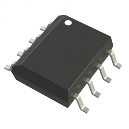
The MC33151DR2G from ON Semiconductor is a dual inverting high-speed MOSFET driver. It is specifically designed for applications that require low current digital circuitry to drive large capacitive loads with high slew rates. The device features low input current, making it compatible with CMOS and LSTTL logic. It also includes input hysteresis for fast output switching, independent of input transition time.
This dual driver offers two high current totem pole outputs, ideally suited for driving power MOSFETs. It operates within a supply voltage range of 6.5V to 18V and provides an output current of 1.5A per channel. The device is available in an 8-pin SOIC package and is suitable for surface mounting.
Typical applications for the MC33151DR2G include switching power supplies, DC-to-DC converters, capacitor charge pump voltage doublers/inverters, and motor controllers. It also includes an undervoltage lockout with hysteresis to prevent erratic system operation at low supply voltages. The device is Pb-Free and Halide-Free.
The MC33151DR2G has a peak output current of 1.5A for both source and sink.
The operating supply voltage range is 6.5V to 18V.
The typical rise and fall times are 31ns and 32ns, respectively, according to the manufacturer's page. The datasheet specifies 15ns with a 1000 pF load.
The MC33151DR2G is available in an 8-SOIC package.
The operating junction temperature range is -40°C to 150°C.
Yes, the MC33151DR2G is RoHS3 compliant.
The Moisture Sensitivity Level (MSL) is 1.