

| Distributor | Stock | Pricing | MOQ | PKG | Lead Time | Date Code | On Order Quantity | On Order Delivery | |
|---|---|---|---|---|---|---|---|---|---|
|
1,584 pcs
|
1584 pcs | On Request | 1 | On Request | On Request | 0028+ | On Request | On Request | |
|
100 pcs
|
100 pcs | On Request | 1 | On Request | On Request | On Request | On Request | On Request |
| Category | |
| Manufacturer Name | |
| Lead Spacing | |
| Lead Style | |
| Output Current | |
| Power Dissipation | |
| SVHC Present | |
| Storage Temperature | |
| Tape & Reel |
The MC14049UBD is a Hex Buffer IC manufactured by Motorola Semiconductor. This complementary MOS device is designed for applications requiring low power dissipation and high noise immunity. It supports a wide supply voltage range from 3.0 V to 18 V, allowing for flexible integration into various designs.
The device features a broad operating temperature range, from -55 °C to +125 °C, making it suitable for demanding environments. The input voltage can exceed the VDD supply voltage, facilitating logic-level conversions. It can drive two TTL/DTL loads when used as a CMOS-to-TTL/DTL converter with VDD = 5.0 V.
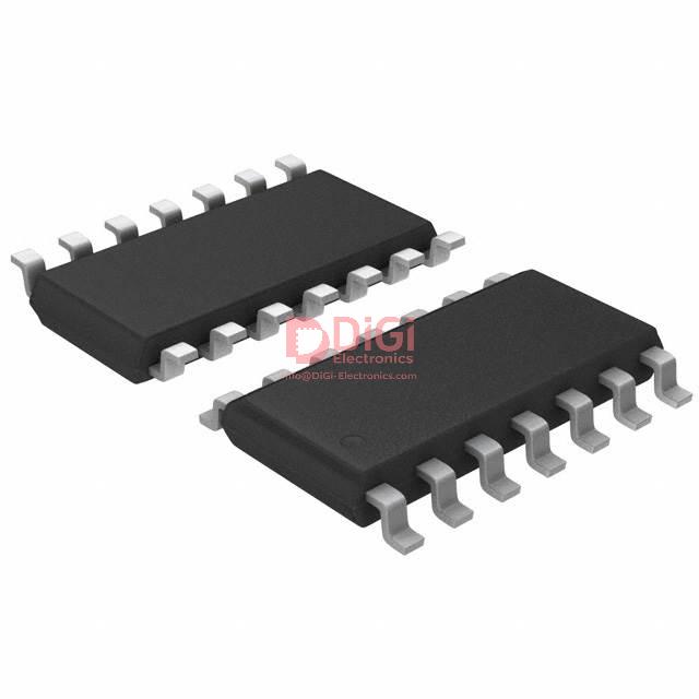
The MC14049UBD comes in a PDIP-16 package. It is constructed with P-channel and N-channel enhancement mode devices in a single monolithic structure. Unused inputs should be tied to an appropriate logic voltage level (VSS or VDD), and unused outputs should be left open.
| Qty | Low | High |
|---|---|---|
| 1+ | $0.22 | $0.22 |
Estimated market price range - modelled values for guidance only, not live distributor offers.
The DC supply voltage range is 3.0V to 18V.
The ambient operating temperature range is -55°C to +125°C.
The device is packaged in a PDIP-16 package.
The maximum output current per pin is +45 mA.
The input voltage range is -0.5V to 18V.
The storage temperature range is -65°C to +150°C.
The maximum power dissipation is 825 mW for the plastic SOIC package.