

| Distributor | Stock | Pricing | MOQ | PKG | Lead Time | Date Code | On Order Quantity | On Order Delivery | |
|---|---|---|---|---|---|---|---|---|---|
|
3,000 pcs
|
3000 pcs | On Request | 1 | On Request | On Request | On Request | On Request | On Request | |
|
1,000 pcs
|
1000 pcs | On Request | 1 | On Request | On Request | On Request | On Request | On Request |
| Category | |
| Manufacturer Name | |
| Current | |
| Input Logic Level | |
| Logic Type | |
| Max Propagation Delay @ V, Max CL | |
| Mounting Type | |
| Number of Circuits | |
| Number of Inputs | |
| Operating Temperature | |
| Power Dissipation | |
| SVHC Present | |
| Supplier Device Package | |
| Voltage |
The MC14001BDG from ON Semiconductor is a high-performance CMOS quad 2-input NOR gate. This device is constructed using P and N channel enhancement mode devices in a single monolithic structure, offering complementary MOS technology. Its primary applications benefit from low power dissipation and high noise immunity.
The gate features a wide supply voltage range from 3.0 Vdc to 18 Vdc. All outputs are buffered, and the device is capable of driving two low-power TTL loads or one low-power Schottky TTL load over the rated temperature range. The operating temperature spans from -55°C to +125°C, making it suitable for demanding environments.
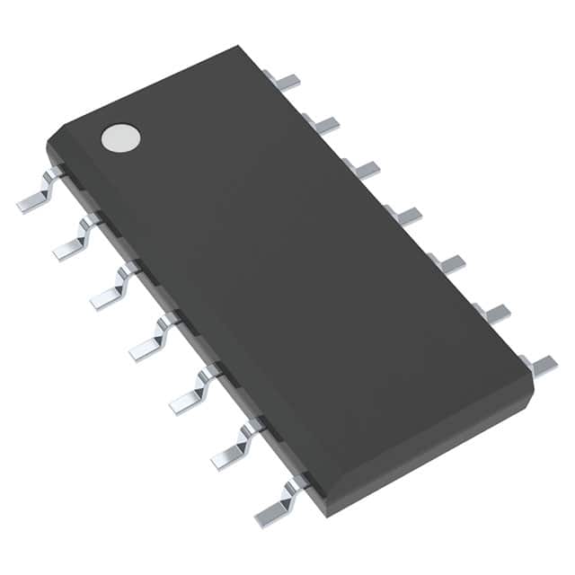
This IC includes double diode protection on all inputs. It is pin-for-pin compatible with corresponding CD4000 Series B Suffix devices. The MC14001BDG is supplied in a 14-SOIC package, designed for surface mounting.
Key electrical characteristics include a maximum propagation delay of 80ns at 15V and 50pF, and a maximum power dissipation of 500 mW per package. The input logic level ranges from 3.5V to 11V.
| Qty | Low | High |
|---|---|---|
| 1+ | $0.22 | $0.22 |
Estimated market price range - modelled values for guidance only, not live distributor offers.
The MC14001BDG operates from 3.0 Vdc to 18 Vdc.
The operating temperature range is -55°C to 125°C.
The MC14001BDG is available in a 14-SOIC surface-mount package.
The maximum propagation delay is 80 ns at 15 V and 50 pF load.
The maximum power dissipation is 500 mW per package.
The ESD withstand voltage is greater than 3000 V.
The maximum input or output current is ±10 mA.