

| Distributor | Stock | Pricing | MOQ | PKG | Lead Time | Date Code | On Order Quantity | On Order Delivery | |
|---|---|---|---|---|---|---|---|---|---|
|
2,080 pcs
|
2080 pcs | On Request | 1 | On Request | On Request | 24+ | On Request | On Request | |
|
181 pcs
|
181 pcs | On Request | 1 | On Request | On Request | On Request | On Request | On Request |
| Category | |
| Manufacturer Name | |
| Current | |
| Frequency | |
| Function | |
| Mounting Type | |
| Number of Outputs | |
| Operating Temperature | |
| Output Configuration | |
| Output Type | |
| Supplier Device Package | |
| Supplier Package | |
| Synchronous Rectifier | |
| Topology | |
| Voltage |
The MAX889TESA+ is a high-frequency, regulated, inverting charge pump IC designed by Analog Devices / Maxim Integrated. It provides a regulated negative output voltage at loads up to 200mA, with an input voltage range from 2.7V to 5.5V.
This device features an adjustable regulated output from -2.5V to -VIN and operates at a switching frequency of up to 2MHz, allowing for the use of small capacitors. It includes a logic-controlled shutdown mode with a low quiescent current of 0.1µA. The MAX889TESA+ also offers soft-start, foldback current limiting, short-circuit protection, and thermal shutdown protection.
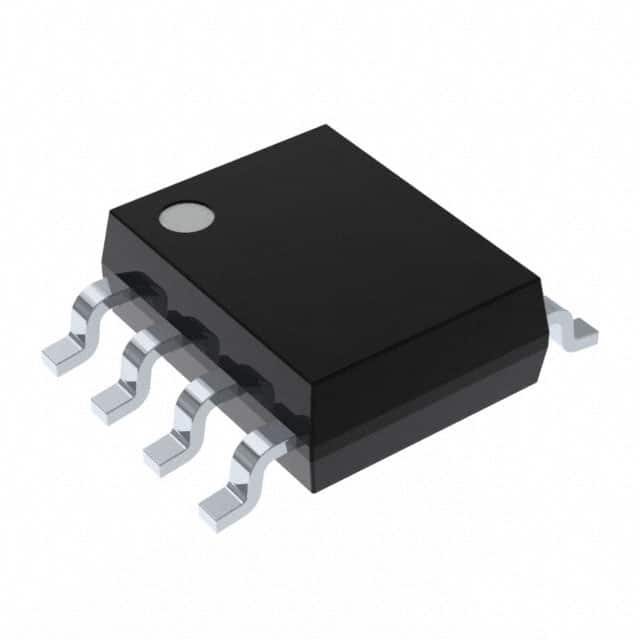
Packaged in an 8-pin SOIC, the MAX889TESA+ is suitable for space-limited applications. Its features make it ideal for use in TFT panels, hard disk drives, camcorders, digital cameras, measurement instruments, and other battery-powered applications.
The device has an output resistance of 0.05Ω in regulation and is available in an 8-pin SO package, supporting surface mount installation.
| Qty | Low | High |
|---|---|---|
| 1+ | $1.08 | $1.08 |
Estimated market price range - modelled values for guidance only, not live distributor offers.
The input voltage range is 2.7V to 5.5V.
The MAX889TESA+ is available in an 8-SOIC surface mount package.
-40°C to +85°C.
200mA.
2MHz.
0.05Ω.
0.1µA.