

| Distributor | Stock | Pricing | MOQ | PKG | Lead Time | Date Code | On Order Quantity | On Order Delivery | |
|---|---|---|---|---|---|---|---|---|---|
|
31 pcs
|
31 pcs | On Request | 1 | On Request | On Request | 2026-02-25 06:16:38 | On Request | On Request |
| Category | |
| Manufacturer Name | |
| Current | |
| Frequency | |
| Function | |
| Input Voltage | |
| Mounting Type | |
| Number of Outputs | |
| Operating Temperature | |
| Output Configuration | |
| Output Type | |
| Quiescent Current | |
| Supplier Device Package | |
| Synchronous Rectifier | |
| Topology | |
| Voltage |
The MAX682ESA+ is a charge pump regulator from Analog Devices, delivering a regulated 5V output with up to 250mA of current from an input voltage range of 2.7V to 5.5V. This device is designed for high-efficiency auxiliary power supplies in applications requiring a compact design, such as battery-powered equipment and miniature electronics.
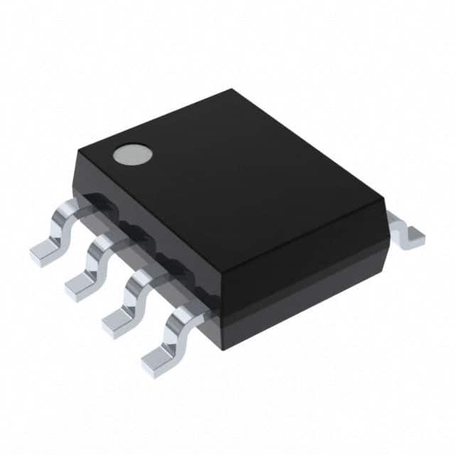
Key features include the absence of inductors, requiring only one resistor and three external capacitors. It operates with adjustable switching frequencies from 50kHz to 2MHz, allowing for the use of small capacitors as low as 1µF per 100mA of output current. The MAX682ESA+ is housed in an 8-pin SOIC package, suitable for surface mounting.
Applications for this charge pump regulator include flash memory supplies, PCMCIA cards, and local 3.3V to 5V conversion. Its compact size and efficient operation make it a versatile solution for power management in space-constrained designs.
| Qty | Low | High |
|---|---|---|
| 1+ | $1.08 | $1.08 |
Estimated market price range - modelled values for guidance only, not live distributor offers.
The input voltage range for the MAX682ESA+ is 2.7V to 5.5V.
The MAX682ESA+ can deliver a maximum output current of 250mA.
The MAX682ESA+ provides a fixed 5V output voltage.
The operating temperature range for the MAX682ESA+ is -40°C to 85°C.
The MAX682ESA+ is available in an 8-SOIC package.
The switching frequency of the MAX682ESA+ is adjustable from 50kHz to 2MHz.