

| Distributor | Stock | Pricing | MOQ | PKG | Lead Time | Date Code | On Order Quantity | On Order Delivery | |
|---|---|---|---|---|---|---|---|---|---|
|
7,147 pcs
|
7147 pcs | On Request | 1 | On Request | On Request | On Request | On Request | On Request |
| Category | |
| Manufacturer Name | |
| Differential | |
| Frequency | |
| Input | |
| Lead Spacing | |
| Mounting Type | |
| Number of Circuits | |
| Operating Temperature | |
| Output | |
| Ratio | |
| Supplier Device Package | |
| Tape & Reel | |
| Type | |
| Voltage |
The Renesas LV810FILF is an integrated circuit functioning as a clock fanout buffer, also known as a clock distribution IC. It is designed to take a single input clock signal and distribute it to ten outputs, providing a 1:10 ratio.
This device supports a maximum operating frequency of 133MHz and features TTL compatible outputs. The operating voltage range is specified from 1.425V to 2.625V, making it suitable for various low-voltage applications. The operating temperature range is -40°C to 85°C.
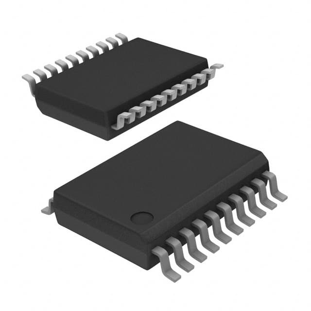
The LV810FILF is packaged in a 20-SSOP (Small Outline Package) with a surface mount type, suitable for automated assembly processes. The package dimensions are 0.154 inches (3.90mm) in width. It is supplied on tape and reel for high-volume manufacturing.
This component is RoHS3 compliant and has a Moisture Sensitivity Level (MSL) of 1, indicating it is not sensitive to ambient moisture under typical conditions. The REACH status is unaffected.
| Qty | Low | High |
|---|---|---|
| 1+ | $3.00 | $3.00 |
Estimated market price range - modelled values for guidance only, not live distributor offers.
The maximum operating frequency for the LV810FILF is 133MHz.
The voltage supply range for the LV810FILF is 1.425V to 2.625V.
The LV810FILF provides TTL output signals.
The operating temperature range for the LV810FILF is -40°C to 85°C.
The LV810FILF is supplied in a 20-SSOP package.
The input to output ratio of the LV810FILF is 1:10.
Yes, this part is RoHS3 compliant.