

| Distributor | Stock | Pricing | MOQ | PKG | Lead Time | Date Code | On Order Quantity | On Order Delivery | |
|---|---|---|---|---|---|---|---|---|---|
|
2,568 pcs
|
2568 pcs | On Request | 1 | On Request | On Request | On Request | On Request | On Request |
| Category | |
| Manufacturer Name | |
| Architecture | |
| Configuration | |
| Data Interface | |
| Features | |
| Input Type | |
| Mounting Type | |
| Number of A | |
| Number of Bits | |
| Number of Channels | |
| Number of Inputs | |
| Operating Temperature | |
| Ratio | |
| Reference Type | |
| Sampling Rate (Per Second) | |
| Supplier Device Package | |
| Supply Voltage | |
| Voltage |
The LTC2217IUP is a high-performance 16-bit Analog to Digital Converter (ADC) from Analog Devices, capable of sampling at 105Msps. Designed for digitizing high frequency, wide dynamic range signals, it features an input frequency range up to 400MHz and a fixed input range of 2.75Vp-p.
This ADC excels in demanding communications applications, boasting an 81.3dBFS noise floor and 100dB spurious free dynamic range (SFDR). Its ultra-low jitter of 85fsRMS allows for effective undersampling of high input frequencies while maintaining excellent noise performance. Key DC specifications include ±3.5LSB INL and ±1LSB DNL (no missing codes).
The digital output can be configured as either differential LVDS or single-ended CMOS. The CMOS outputs offer flexibility with two format options: a single bus at full data rate or demultiplexed buses at half data rate. A separate output power supply allows the CMOS output swing to range from 0.5V to 3.6V. The device operates from a single 3.3V supply and has a typical power dissipation of 1.19W.
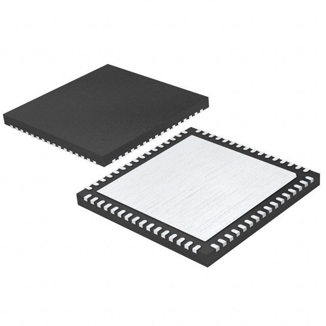
Packaged in a 64-QFN (9x9mm) format, the LTC2217IUP is suitable for surface mount applications. It is designed for use in telecommunications, receivers, cellular base stations, spectrum analysis, imaging systems, and ATE.
The LTC2217IUP has a maximum sample rate of 105Msps.
The typical noise floor of the LTC2217IUP is -81.3dBFS.
The LTC2217IUP offers a spurious free dynamic range (SFDR) of 100dB, and greater than 90dB at 70MHz.
The typical input range for the LTC2217IUP is 2.75Vp-p.
The LTC2217IUP operates in a temperature range of -40°C to 85°C.
The LTC2217IUP is available in a 64-QFN (9x9mm) package suitable for surface mounting.