

| Distributor | Stock | Pricing | MOQ | PKG | Lead Time | Date Code | On Order Quantity | On Order Delivery | |
|---|---|---|---|---|---|---|---|---|---|
|
493 pcs
|
493 pcs | On Request | 1 | On Request | On Request | 15+ | On Request | On Request |
| Category | |
| Manufacturer Name | |
| Interface | |
| Lead Spacing | |
| Lead Style | |
| SVHC Present |
The LT3965/LT3965-1 is an LED bypass switching device for dimming individual LEDs in a string using a common current source. It features eight individually controlled floating source 17V/330mΩ NMOS switches. The eight switches can be connected in parallel and/or in series to bypass current around one or more LEDs in a string.
The device utilizes an I2C serial interface for communication with a microcontroller. Each of the eight channels can be independently programmed for constant on/off, or PWM dimming with or without fade transition. The fade option provides 11-bit resolution logarithmic transition between PWM dimming states. The LT3965/LT3965-1 supports both an internal clock generator and an external clock source for PWM dimming.
Key features include independent on/off/dimming control for up to 4 LEDs per switch, I2C multidrop serial interface with programmable fault reporting for open and shorted LEDs, and 16 unique I2C addresses. The VDD range is 2.7V to 5.5V, and the VIN range is 8V to 60V. It offers digital programmable 256:1 PWM dimming and flicker-free PWM dimming. The device is AEC-Q100 qualified for automotive applications.
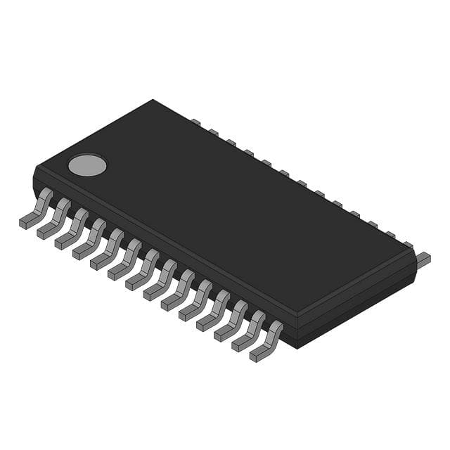
The LT3965EFE#PBF is available in a 28-lead TSSOP package.
| Qty | Low | High |
|---|---|---|
| 1+ | $0.17 | $0.17 |
Estimated market price range - modelled values for guidance only, not live distributor offers.
The switches are rated for 17V.
The on-resistance is 330mΩ.
The VDD operating voltage range is 2.7V to 5.5V.
The VIN voltage range is 8V to 60V.
The PWM dimming resolution is digitally programmable at 256:1.
This device uses an I2C serial interface.
The LT3965EFE#PBF is available in a 28-lead TSSOP package.