

| Distributor | Stock | Pricing | MOQ | PKG | Lead Time | Date Code | On Order Quantity | On Order Delivery | |
|---|---|---|---|---|---|---|---|---|---|
|
900 pcs
|
900 pcs | On Request | 1 | On Request | On Request | On Request | On Request | On Request | |
|
245 pcs
|
245 pcs | On Request | 1 | On Request | On Request | On Request | On Request | On Request |
| Category | |
| Manufacturer Name | |
| Differential | |
| Frequency | |
| Input | |
| Input Type | |
| Mounting Type | |
| Number of Circuits | |
| Number of Outputs | |
| Operating Temperature | |
| Output | |
| Output Type | |
| Ratio | |
| Slew Rate | |
| Supplier Device Package | |
| Type | |
| Voltage |
The LMV112SD/NOPB is a high-speed dual clock buffer designed by Texas Instruments for portable communications and accurate multi-clock systems. It integrates two 40 MHz low-noise buffers, optimizing applications and outperforming larger discrete solutions.
This device enables superb system operation between the baseband and the oscillator signal path while eliminating crosstalk. It offers a supply voltage range of 2.4V to 5V and operates within a temperature range of -40°C to 85°C. The LMV112SD/NOPB features rail-to-rail input and output, individual buffer enable pins, and a slew rate of 110 V/µs.
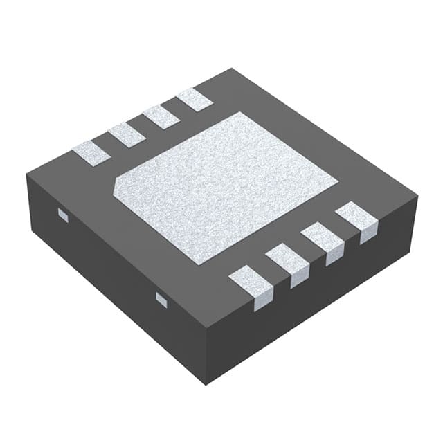
Packaged in an 8-WSON (3x3 mm) surface-mount package, the LMV112SD/NOPB is suitable for space-constrained designs. Its low power consumption makes it ideal for battery-powered applications. The robust, independent, and flexible buffers are designed to manage complex clock signals in wireless applications.
Key electrical characteristics include a small signal bandwidth of 40 MHz, a total supply current of 1.6 mA, and a shutdown current of 59 µA. The device supports individual enable pin controls and can operate with single or split supplies.
| Qty | Low | High |
|---|---|---|
| 1+ | $0.85 | $0.85 |
Estimated market price range - modelled values for guidance only, not live distributor offers.
The LMV112SD/NOPB operates within a supply voltage range of 2.4V to 5V.
The operating temperature range for the LMV112SD/NOPB is -40°C to 85°C.
The LMV112SD/NOPB is supplied in an 8-WSON (3x3 mm) package.
The LMV112SD/NOPB is RoHS3 Compliant.