

| Distributor | Stock | Pricing | MOQ | PKG | Lead Time | Date Code | On Order Quantity | On Order Delivery | |
|---|---|---|---|---|---|---|---|---|---|
|
1,000 pcs
|
1000 pcs | On Request | 1 | On Request | On Request | On Request | On Request | On Request |
| Category | |
| Manufacturer Name | |
| Differential | |
| Frequency | |
| Input | |
| Lead Spacing | |
| Mounting Type | |
| Number of Circuits | |
| Operating Temperature | |
| Output | |
| Propagation Delay | |
| Ratio | |
| Supplier Device Package | |
| Type | |
| Voltage |
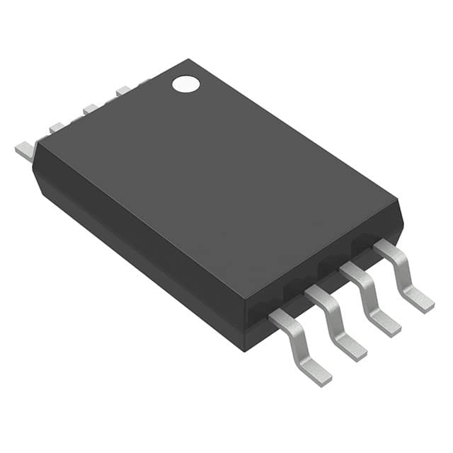
The LMK1C1103PWR is a 1:3 LVCMOS clock buffer from Texas Instruments, part of the LMK1C110x family. This device is designed for high-performance clock distribution, featuring very low output skew of less than 50 ps and extremely low additive jitter of less than 50 fs.
It supports supply voltages of 1.8 V, 2.5 V, and 3.3 V, with a 3.3-V tolerant input across all supply voltages. The maximum operating frequency is 250 MHz at 3.3 V and 200 MHz at 2.5 V and 1.8 V. The operating temperature range is -40°C to 125°C.
This clock buffer is available in an 8-pin TSSOP package and is suitable for applications requiring precise clock signal distribution, such as factory automation, telecommunications equipment, and data center computing.
The LMK1C110x family offers modularity and pin compatibility, designed for easy integration into existing designs. It includes fail-safe inputs to prevent oscillation and a synchronous output enable control.
| Qty | Low | High |
|---|---|---|
| 1+ | $0.96 | $0.96 |
Estimated market price range - modelled values for guidance only, not live distributor offers.
The maximum operating frequency is 250 MHz for 3.3 V and 200 MHz for 2.5 V and 1.8 V.
The output skew is less than 50 ps.
The additive jitter is less than 50 fs maximum.
It supports supply voltages of 1.8 V, 2.5 V, and 3.3 V.
The operating temperature range is -40°C to 125°C.
The LMK1C1103PWR is available in an 8-TSSOP package.