
BC847B/215
Nexperia USA Inc.
The Nexperia USA Inc. BC847B/215 is a bipolar transistor. It is RoHS3 Compliant and has an MSL Level 1 rating.


| Distributor | Stock | Pricing | MOQ | PKG | Lead Time | Date Code | On Order Quantity | On Order Delivery | |
|---|---|---|---|---|---|---|---|---|---|
|
4,520 pcs
|
4520 pcs | On Request | 1 | On Request | On Request | On Request | On Request | On Request |
| Category | |
| Manufacturer Name | |
| SVHC Present |
The LMK00304SQ from Texas Instruments is a high-performance differential clock buffer and level translator designed for demanding high-frequency applications. It features a 3.1-GHz maximum input frequency and supports a variety of input signal types including LVPECL, LVDS, CML, SSTL, HSTL, HCSL, and single-ended clocks. The device offers a 3:1 input multiplexer and a crystal input that accepts frequencies from 10 MHz to 40 MHz.
This clock buffer provides two banks, each with two differential outputs that are selectable between LVPECL, LVDS, HCSL, or Hi-Z states. It boasts very low additive jitter, with typical values of 20 fs RMS (10 kHz to 1 MHz) and 51 fs RMS (12 kHz to 20 MHz) when used with an LMK03806 clock source at 156.25 MHz. High Power Supply Rejection Ratio (PSRR) is also a key feature, with -65 dBc for LVPECL and -76 dBc for LVDS at 156.25 MHz.
The LMK00304SQ supports a core supply voltage of 3.3 V ± 5% and three independent VCCO output supplies of 3.3 V or 2.5 V ± 5%. Configuration is managed via pin control, and it includes an LVCMOS output with a synchronous enable input. The device operates within an industrial temperature range of -40°C to +85°C.
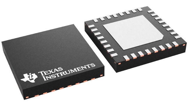
Packaged in a 32-lead WQFN (5 mm x 5 mm) with surface mount termination, the LMK00304SQ is suitable for various high-frequency timing distribution needs.
| Qty | Low | High |
|---|---|---|
| 1+ | $3.00 | $3.00 |
Estimated market price range - modelled values for guidance only, not live distributor offers.
The LMK00304SQ operates from -40°C to 85°C.
The LMK00304SQ is offered in a 32-lead WQFN (RTV) package measuring 5 mm x 5 mm.
The device features a 3:1 input multiplexer.
The universal inputs operate up to 3.1 GHz.
Each output bank can be configured as LVPECL, LVDS, HCSL, or Hi-Z.
Typical LVPECL additive jitter is 20 fs RMS (10 kHz – 1 MHz) and 51 fs RMS (12 kHz – 20 MHz) with an LMK03806 clock source at 156.25 MHz.
The core supply (VCC) is 3.3 V ±5%, and the output supplies (VCCO) are 3.3 V or 2.5 V ±5%.