

| Distributor | Stock | Pricing | MOQ | PKG | Lead Time | Date Code | On Order Quantity | On Order Delivery | |
|---|---|---|---|---|---|---|---|---|---|
|
8,218 pcs
|
8218 pcs | On Request | 1 | On Request | On Request | On Request | On Request | On Request | |
|
960 pcs
|
960 pcs | On Request | 1 | On Request | On Request | 17+ | On Request | On Request |
| Category | |
| Manufacturer Name | |
| AEC Qualified | |
| Automotive Grade | |
| Differential | |
| Frequency | |
| Industrial Grade | |
| Input | |
| Medical Grade | |
| Military Grade | |
| Mounting Type | |
| Number of Circuits | |
| Number of Outputs | |
| Operating Temperature | |
| Output | |
| Ratio | |
| Supplier Device Package | |
| Tape & Reel | |
| Type | |
| Voltage |
The Texas Instruments LMK00101SQE/NOPB is an ultra-low jitter LVCMOS fanout buffer and level translator. It is capable of distributing 10 clocks with extremely low jitter from a variety of input types, including differential, single-ended, and crystal oscillators.
This buffer features a universal input that supports LVPECL, LVDS, HCSL, SSTL, and LVCMOS/LVTTL signals, as well as crystal inputs from 10 to 40 MHz. It provides 10 LVCMOS/LVTTL outputs operating at frequencies up to 200 MHz. The core supply voltage can be set to 2.5 V or 3.3 V, while the output supply voltage is adjustable from 1.5 V to 3.3 V for each bank.
Designed for high-performance applications, the LMK00101 offers ultra-low skew (25 ps typical) and low additive RMS jitter (30 fs typical). It supports synchronous output enable for glitch-free operation and has a high Power Supply Rejection Ratio (PSRR). These characteristics make it suitable for networking, telecom, server and storage area networking, RRU LO reference distribution, medical, and test equipment applications.
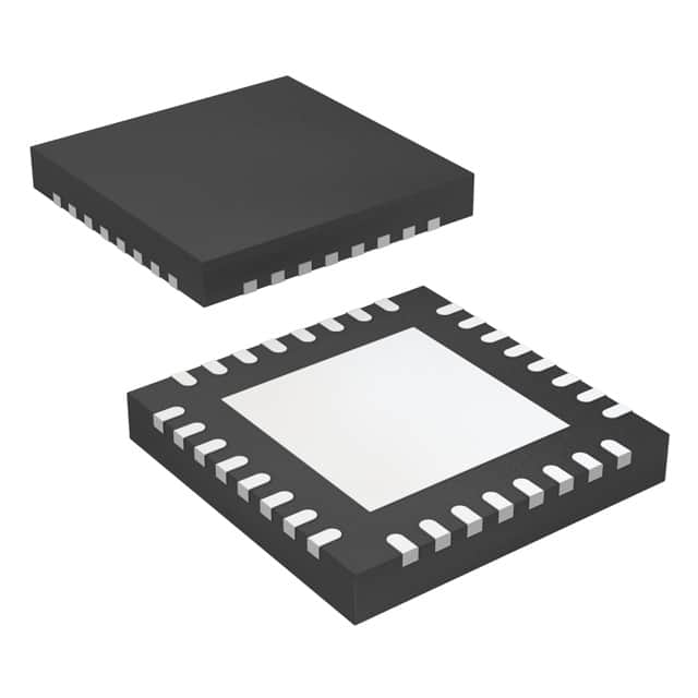
The device is housed in a 32-pin WQFN package measuring 5 mm x 5 mm with an exposed pad. It is designed for surface mount applications and operates within a temperature range of -40°C to 85°C.
| Qty | Low | High |
|---|---|---|
| 1+ | $4.14 | $4.14 |
Estimated market price range - modelled values for guidance only, not live distributor offers.
The operating temperature range is -40°C to 85°C.
It is available in a 32-WQFN (5x5) package and a 32-WFQFN Exposed Pad package.
The output types supported are LVCMOS and LVTTL.
The maximum frequency is 200 MHz.
The typical additive RMS jitter is 30 fs.
The core supply voltage options are 2.5 V and 3.3 V, while the output supply voltage can be set to 1.5 V, 1.8 V, 2.5 V, or 3.3 V.