

| Distributor | Stock | Pricing | MOQ | PKG | Lead Time | Date Code | On Order Quantity | On Order Delivery | |
|---|---|---|---|---|---|---|---|---|---|
|
6,218 pcs
|
6218 pcs | On Request | 1 | On Request | On Request | 23+ | On Request | On Request | |
|
3,480 pcs
|
3480 pcs | On Request | 1 | On Request | On Request | On Request | On Request | On Request | |
|
798 pcs
|
798 pcs | On Request | 1 | On Request | On Request | 22+ | On Request | On Request |
| Category | |
| Manufacturer Name | |
| AEC Qualified | |
| Automotive Grade | |
| Clock Sync | |
| Control Features | |
| Duty Cycle (Max) | |
| Frequency | |
| Function | |
| Mounting Type | |
| Number of Outputs | |
| Operating Temperature | |
| Output Configuration | |
| Output Phases | |
| Output Type | |
| Storage Temperature | |
| Supplier Device Package | |
| Synchronous Rectifier | |
| Tape & Reel | |
| Topology | |
| Voltage |
The LM51551QDSSTQ1 from Texas Instruments is a versatile DC DC switching controller designed for automotive and portable battery applications. It supports Boost, Flyback, and SEPIC topologies, offering flexibility in power supply design.
This controller operates with a wide input voltage range from 1.5V to 45V, making it suitable for various power sources. It can achieve output voltages up to 300V. Key electrical features include a maximum switching frequency of 2.2 MHz, adjustable current limit, and a 1.5A peak MOSFET driver. The device also incorporates features like soft start, frequency synchronization, hiccup mode protection, and power good indication.
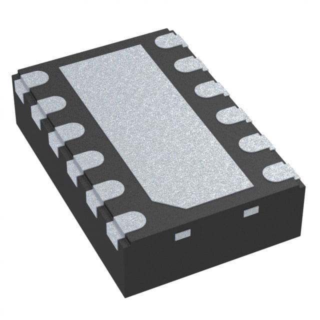
Packaged in a 12-WSON (3x2 mm) with wettable flank options, the LM51551QDSSTQ1 is designed for surface mount applications. It operates within an extended temperature range of -40°C to 150°C (TJ), ensuring reliability in demanding environments. The AEC-Q100 qualification further underscores its suitability for automotive use. Its low quiescent current and shutdown current minimize battery drain, while integrated error amplifier allows for primary-side regulation without an optocoupler in flyback configurations.
| Qty | Low | High |
|---|---|---|
| 1+ | $1.37 | $1.37 |
Estimated market price range - modelled values for guidance only, not live distributor offers.
The LM51551QDSSTQ1 has an input voltage range from 1.5 V to 45 V. When BIAS = VCC, the minimum input voltage is 2.97 V.
The LM51551QDSSTQ1 can provide an output voltage from 1.5 V to 300 V.
The switching frequency of the LM51551QDSSTQ1 ranges from 100 kHz to 2.2 MHz.
The maximum operating junction temperature (TJ) for the LM51551QDSSTQ1 is 150°C. The maximum ambient operating temperature (TA) is 125°C.
The LM51551QDSSTQ1 is available in a 12-WSON (3x2) or 12-WFDFN Exposed Pad package.
The typical quiescent current (Iq) for the LM51551QDSSTQ1 is 480 µA.
The maximum duty cycle for the LM51551QDSSTQ1 is 93%.