

| Distributor | Stock | Pricing | MOQ | PKG | Lead Time | Date Code | On Order Quantity | On Order Delivery | |
|---|---|---|---|---|---|---|---|---|---|
|
2,050 pcs
|
2050 pcs | On Request | 1 | On Request | On Request | 24+ | On Request | On Request | |
|
400 pcs
|
400 pcs | On Request | 1 | On Request | On Request | On Request | On Request | On Request | |
|
6 pcs
|
6 pcs | On Request | 1 | On Request | On Request | 1446 | On Request | On Request |
| Category | |
| Manufacturer Name | |
| Frequency | |
| Mounting Type | |
| Number of I | |
| Number of Logic Elements | |
| Operating Temperature | |
| Supplier Device Package | |
| Supplier Package | |
| Tape & Reel | |
| Technology | |
| Total RAM Bits | |
| Voltage |
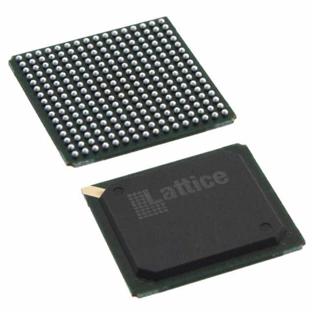
The Lattice LFXP6C-4FN256C is an FPGA from the LatticeXP family, designed for cost-effective system designs. It features a non-volatile, infinitely reconfigurable architecture with instant-on capability, powering up in microseconds without external configuration memory. This device offers 6000 LUT4 logic elements and supports up to 188 I/O pins.
Key electrical specifications include 73728 bits of total RAM, with 22 Kbits of distributed RAM and 72 Kbits of embedded block RAM. It operates within a voltage range of 1.71V to 3.465V and supports up to 4 analog PLLs. The technology node is 130nm, with a maximum frequency of 360MHz.
The LFXP6C-4FN256C comes in a 256-BGA package, specifically a 256-FPBGA (17x17 mm) with surface mount mounting type. It operates between 0°C and 85°C (TJ).
This FPGA supports various I/O interfaces including LVCMOS, LVTTL, SSTL, and HSTL, and includes dedicated DDR memory support up to DDR333. System-level support includes IEEE 1149.1 Boundary Scan and ispTRACY internal logic analyzer capability.
The LFXP6C-4FN256C has 6000 logic elements.
The LFXP6C-4FN256C has 188 I/O pins.
The operating voltage range is 1.71V to 3.465V.
The LFXP6C-4FN256C is supplied in a 256-BGA package.
The operating temperature range is 0°C to 85°C (TJ).
The LFXP6C-4FN256C has a total of 73728 RAM bits.
The technology node is 130nm.