

| Distributor | Stock | Pricing | MOQ | PKG | Lead Time | Date Code | On Order Quantity | On Order Delivery | |
|---|---|---|---|---|---|---|---|---|---|
|
400 pcs
|
400 pcs | On Request | 1 | On Request | On Request | On Request | On Request | On Request |
| Category | |
| Manufacturer Name | |
| Lead Spacing | |
| Mounting Type | |
| Number of I | |
| Number of Logic Elements | |
| Operating Temperature | |
| Supplier Device Package | |
| Tape & Reel | |
| Total RAM Bits | |
| Voltage |
The Lattice Semiconductor LFXP6C-3FN256I is a Field Programmable Gate Array (FPGA) designed for flexible logic implementation. This device offers 6000 logic elements and 188 input/output (I/O) pins, supporting a wide range of interface requirements.
Key electrical characteristics include a total of 73728 RAM bits for embedded memory functions and an operating voltage range from 1.71V to 3.465V. The operating temperature range is specified from -40°C to 100°C (TJ), making it suitable for various environmental conditions.
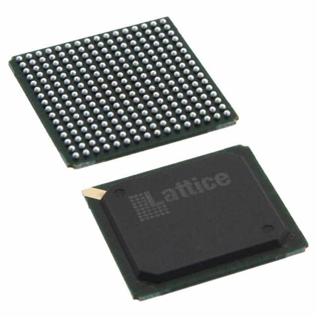
This FPGA is packaged in a 256-BGA (256-FPBGA (17x17)) and utilizes a surface mount configuration. Its non-volatile, infinitely reconfigurable architecture allows for instant-on functionality and in-field logic updates, enhancing design flexibility and security.
The LatticeXP family, to which this device belongs, provides extensive density and package options, supporting density migration. It features programmable I/O buffers supporting multiple interface standards and dedicated DDR memory support.
The LFXP6C-3FN256I FPGA has 6000 logic elements.
The LFXP6C-3FN256I FPGA has 188 I/O pins.
The LFXP6C-3FN256I FPGA operates between 1.71V and 3.465V.
The LFXP6C-3FN256I FPGA is supplied in a 256-BGA package, specifically a 256-FPBGA (17x17).
The LFXP6C-3FN256I FPGA has an operating temperature range of -40°C to 100°C (TJ).
The LFXP6C-3FN256I FPGA contains 73728 bits of total RAM.
The LFXP6C-3FN256I FPGA requires a surface mount type.