
LFXP2-8E-6TN144I
Lattice Semiconductor Corporation
The Lattice Semiconductor LFXP2-8E-6TN144I is an FPGA from the LatticeXP2 family. It features 8000 logic elements and 100 I/O pins.


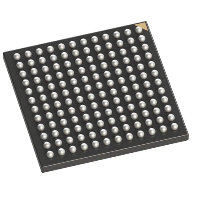
| Distributor | Stock | Pricing | MOQ | PKG | Lead Time | Date Code | On Order Quantity | On Order Delivery | |
|---|---|---|---|---|---|---|---|---|---|
|
15 pcs
|
15 pcs | On Request | 1 | On Request | On Request | On Request | On Request | On Request |
| Category | |
| Manufacturer Name | |
| Mounting Type | |
| Number of I | |
| Number of LABs | |
| Number of Logic Elements | |
| Operating Temperature | |
| Supplier Device Package | |
| Tape & Reel | |
| Total RAM Bits | |
| Voltage |
The Lattice Semiconductor LFXP2-8E-5TN144I is a Field Programmable Gate Array (FPGA) IC from the XP2 family. It offers 8000 logic elements and 100 I/O pins, making it suitable for various embedded applications. The device includes 226304 bits of RAM and operates within a voltage supply range of 1.14V to 1.26V.
This FPGA is designed for surface mounting and comes in a 144-LQFP package, with the supplier device package specified as 144-TQFP (20x20). The operating temperature range is -40°C to 100°C (TJ). Its architecture supports flexible configuration and system-level integration.
The flexiFLASH architecture provides instant-on capability and infinite reconfigurability. Features like FlashBAK technology for embedded block memory and Serial TAG memory for design security are integrated. The device also supports Live Update Technology with TransFR technology and secure updates via 128-bit AES encryption.
The LFXP2-8E-5TN144I has 8000 logic elements.
The LFXP2-8E-5TN144I has 100 I/O pins.
The operating voltage for the LFXP2-8E-5TN144I is between 1.14V and 1.26V.
The LFXP2-8E-5TN144I is available in a 144-LQFP package, with the supplier device package being 144-TQFP (20x20).
The operating temperature range for the LFXP2-8E-5TN144I is -40°C to 100°C (TJ).
The LFXP2-8E-5TN144I has a total of 226304 RAM bits.