

| Distributor | Stock | Pricing | MOQ | PKG | Lead Time | Date Code | On Order Quantity | On Order Delivery | |
|---|---|---|---|---|---|---|---|---|---|
|
1,077 pcs
|
1077 pcs | On Request | 1 | On Request | On Request | On Request | On Request | On Request |
| Category | |
| Manufacturer Name | |
| Lead Spacing | |
| Mounting Type | |
| Number of I | |
| Number of LABs | |
| Number of Logic Elements | |
| Operating Temperature | |
| Operating Voltage | |
| Supplier Device Package | |
| Total RAM Bits | |
| Voltage |
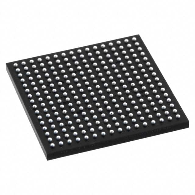
The Lattice LFXP2-8E-5FTN256I is a Field Programmable Gate Array (FPGA) belonging to the LatticeXP2 family. This device utilizes the flexiFLASH architecture, offering instant-on capability and infinite reconfigurability. It provides 8000 LUTs (Logic Elements) and 1000 Logic Array Blocks (LABs), along with 226304 bits of embedded memory (sysMEM EBR) and up to 83 Kbits of distributed RAM.
Key electrical features include a 1.2V operating voltage and 201 I/O pins supporting various buffer standards. The device also incorporates up to four sysCLOCK PLLs for clock management and sysDSP blocks for high-performance multiply-accumulate operations. The operating temperature range is -40°C to 100°C (TJ).
This FPGA is available in a 256-FTBGA (17x17 mm) package, suitable for surface mount applications. It supports SPI boot flash interface and dual boot images, enhancing device configuration flexibility. The LatticeXP2 family is designed for a wide range of applications requiring flexible, non-volatile programmable logic solutions.
The LFXP2-8E-5FTN256I FPGA has 8000 logic elements.
The LFXP2-8E-5FTN256I FPGA has 201 I/O pins.
The LFXP2-8E-5FTN256I FPGA operates at 1.14V to 1.26V.
The LFXP2-8E-5FTN256I FPGA is supplied in a 256-FTBGA (17x17) package.
The operating temperature range for the LFXP2-8E-5FTN256I FPGA is -40°C to 100°C (TJ).
The LFXP2-8E-5FTN256I FPGA has a total of 226304 RAM bits.
Yes, the LFXP2-8E-5FTN256I FPGA features flexiFLASH architecture which provides instant-on capability.