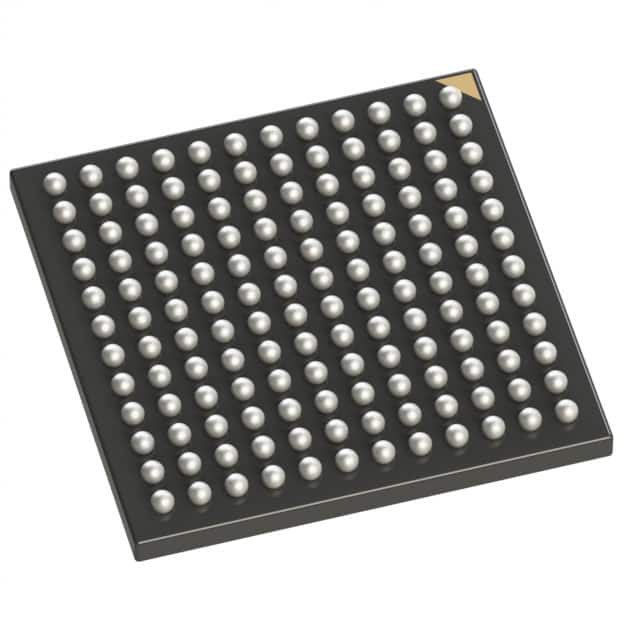
The Lattice Semiconductor LFXP2-5E-6TN144C is a Field Programmable Gate Array (FPGA) from the LatticeXP2 family. It features a flexiFLASH architecture providing instant-on capability and infinite reconfigurability.
This FPGA offers 5000 LUTs (Look-Up Tables) and supports up to 100 I/O pins. It includes 169984 total RAM bits and operates within a voltage range of 1.14V to 1.26V. The device is designed for surface mounting and comes in a 144-TQFP package.
Key features include sysDSP blocks for high-performance multiply and accumulate operations, sysCLOCK PLLs for clock management, and flexible I/O buffers supporting various standards like LVCMOS, LVTTL, SSTL, and HSTL. It also supports pre-engineered source synchronous interfaces such as DDR/DDR2 up to 200 MHz and 7:1 LVDS interfaces.
The LatticeXP2 family is known for its embedded memory capabilities, including sysMEM EBR and Distributed RAM. The device is compliant with IEEE 1149.1 and IEEE 1532 standards, and operates with a 1.2V power supply.