

| Distributor | Stock | Pricing | MOQ | PKG | Lead Time | Date Code | On Order Quantity | On Order Delivery | |
|---|---|---|---|---|---|---|---|---|---|
|
1,511 pcs
|
1511 pcs | On Request | 1 | On Request | On Request | 16+ | On Request | On Request |
| Category | |
| Manufacturer Name | |
| Mounting Style | |
| Mounting Type | |
| Number of I | |
| Number of LABs | |
| Number of Logic Elements | |
| Operating Temperature | |
| Operating Voltage | |
| Supplier Device Package | |
| Tape & Reel | |
| Total RAM Bits | |
| Voltage |
The Lattice LFXP2-5E-5FT256I is a Field Programmable Gate Array (FPGA) from the LatticeXP2 family. It features a flexiFLASH architecture providing instant-on capability and infinite reconfigurability. This device offers 5000 logic elements (LUTs) and supports up to 172 I/O pins.
Key technical specifications include 625 Logic Array Blocks (LABs) and a total RAM bit count of 169,984. It also provides 10 Kbit of Distributed RAM and 166 Kbit of Embedded Block RAM (EBR). The operating supply voltage ranges from 1.14V to 1.26V, with a typical value of 1.2V. The operating temperature range is -40°C to 100°C (TJ).
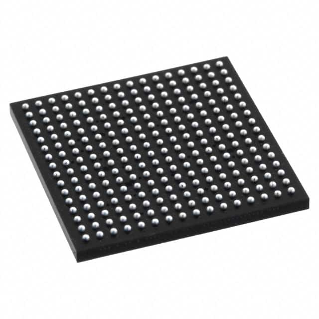
This FPGA is housed in a 256-FTBGA (17x17 mm) package, also referred to as 256-LBGA. It is designed for surface mount (SMD/SMT) applications and is supplied in a tray. The LatticeXP2 family supports features like sysDSP blocks for high-performance multiply-accumulate operations, sysCLOCK PLLs for clock management, and flexible I/O buffers supporting various standards.
With its combination of non-volatile Flash technology and FPGA fabric, the LFXP2-5E-5FT256I is suitable for a wide range of embedded applications requiring flexible logic implementation and instant-on functionality.
The LFXP2-5E-5FT256I has 5000 logic elements.
The LFXP2-5E-5FT256I has 172 I/O pins.
The operating supply voltage for the LFXP2-5E-5FT256I is between 1.14V and 1.26V.
The LFXP2-5E-5FT256I is supplied in a 256-FTBGA (17x17 mm) package.
The operating temperature range for the LFXP2-5E-5FT256I is -40°C to 100°C (TJ).
The LFXP2-5E-5FT256I has a total of 169,984 RAM bits.