

| Distributor | Stock | Pricing | MOQ | PKG | Lead Time | Date Code | On Order Quantity | On Order Delivery | |
|---|---|---|---|---|---|---|---|---|---|
|
50 pcs
|
50 pcs | On Request | 1 | On Request | On Request | On Request | On Request | On Request |
| Category | |
| Manufacturer Name | |
| Lead Spacing | |
| Mounting Type | |
| Number of I | |
| Number of LABs | |
| Number of Logic Elements | |
| Operating Temperature | |
| Supplier Device Package | |
| Tape & Reel | |
| Total RAM Bits | |
| Voltage |
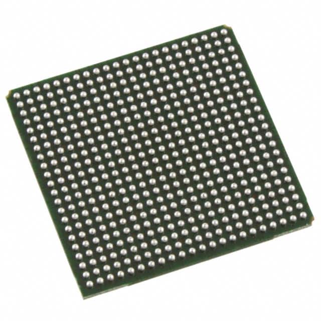
The Lattice Semiconductor LFXP2-40E-6FN484C is a Field Programmable Gate Array (FPGA) from the LatticeXP2 family. It features a flexiFLASH architecture providing instant-on capability and infinite reconfigurability. This device offers 40,000 logic elements and supports up to 363 I/O pins.
Key electrical specifications include an operating voltage range of 1.14V to 1.26V and an operating temperature range of 0°C to 85°C (TJ). The FPGA is equipped with 906,240 bits of total RAM and 5,000 LABs. It is housed in a 484-BBGA package, with the supplier specifying a 484-FPBGA (23x23) package.
The device supports surface mount mounting. It is designed for applications requiring flexible and reconfigurable logic solutions. The LatticeXP2 family is known for its embedded memory and DSP blocks, making it suitable for various digital signal processing tasks.
The LFXP2-40E-6FN484C has 40,000 logic elements.
The LFXP2-40E-6FN484C has 363 I/O pins.
The operating voltage range is 1.14V to 1.26V.
It is supplied in a 484-BBGA package, specifically a 484-FPBGA (23x23).
The operating temperature range is 0°C to 85°C (TJ).