

| Distributor | Stock | Pricing | MOQ | PKG | Lead Time | Date Code | On Order Quantity | On Order Delivery | |
|---|---|---|---|---|---|---|---|---|---|
|
25 pcs
|
25 pcs | On Request | 1 | On Request | On Request | On Request | On Request | On Request |
| Category | |
| Manufacturer Name | |
| Mounting Type | |
| Number of I | |
| Number of LABs | |
| Number of Logic Elements | |
| Operating Temperature | |
| Operating Voltage | |
| Supplier Device Package | |
| Supplier Package | |
| Tape & Reel | |
| Total RAM Bits | |
| Voltage |
The LFXP2-30E-7FTN256C is a Field Programmable Gate Array (FPGA) from Lattice Semiconductor, part of the XP2 series. This device features a flexiFLASH architecture, offering instant-on capability and infinite reconfigurability.
Key specifications include 29,000 logic cells and 3,625 LABs/CLBs, providing substantial capacity for complex digital designs. It offers 396,288 total RAM bits for embedded memory operations and supports 201 I/O pins for extensive interfacing. The device operates with a supply voltage between 1.14V and 1.26V and has an operating temperature range of 0°C to 85°C (TJ).
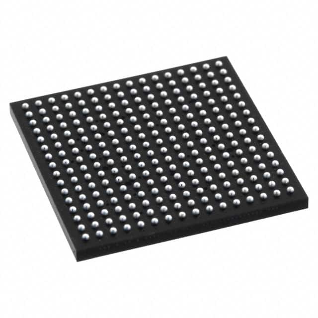
This FPGA is housed in a 256-FTBGA package, suitable for surface mount applications. The flexiFLASH architecture utilizes non-volatile flash configuration, eliminating the need for external configuration memory and enabling fast startup times. Its design supports embedded systems, signal processing, industrial control, communications hardware, and consumer electronics.
The LatticeXP2 family, to which this part belongs, emphasizes features like sysDSP blocks for high-performance multiply-accumulate operations, sysCLOCK PLLs for flexible clock management, and sysIO buffers supporting various I/O standards. The device operates with a 1.2V power supply, contributing to low power consumption.
The LFXP2-30E-7FTN256C FPGA has 29,000 logic elements.
The LFXP2-30E-7FTN256C FPGA offers 201 I/O pins.
The LFXP2-30E-7FTN256C FPGA operates within a supply voltage range of 1.14V to 1.26V.
The LFXP2-30E-7FTN256C FPGA is supplied in a 256-FTBGA package.
The LFXP2-30E-7FTN256C FPGA operates between 0°C and 85°C (TJ).
The LFXP2-30E-7FTN256C FPGA has a total of 396,288 RAM bits.
The LFXP2-30E-7FTN256C FPGA has 3,625 LABs/CLBs.