

| Distributor | Stock | Pricing | MOQ | PKG | Lead Time | Date Code | On Order Quantity | On Order Delivery | |
|---|---|---|---|---|---|---|---|---|---|
|
10 pcs
|
10 pcs | On Request | 1 | On Request | On Request | On Request | On Request | On Request |
| Category | |
| Manufacturer Name | |
| Mounting Type | |
| Number of I | |
| Number of LABs | |
| Number of Logic Elements | |
| Operating Temperature | |
| Package / Case | |
| Supplier Device Package | |
| Tape & Reel | |
| Total RAM Bits | |
| Voltage |
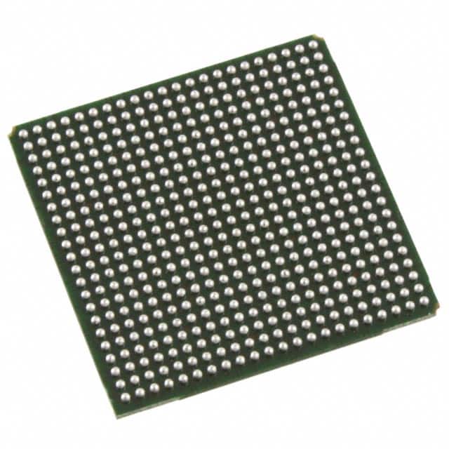
The Lattice Semiconductor LFXP2-17E-7FN484C is a Field Programmable Gate Array (FPGA) from the LatticeXP2 family. It features a flexiFLASH architecture, offering instant-on capability and infinite reconfigurability. This device provides 17,000 logic elements and supports 358 I/O pins, with a total RAM bit count of 282,624.
The operating voltage for this FPGA ranges from 1.14V to 1.26V, with an operating temperature range of 0°C to 85°C (TJ). It is housed in a 484-FPBGA (23x23mm) package, with a surface mount type. The device also includes sysDSP blocks for high-performance multiply and accumulate operations, and sysCLOCK PLLs for clock management.
Key features include support for SPI boot flash interface, dual boot image capability, and on-chip oscillator. The flexible I/O buffer supports various standards including LVCMOS, SSTL, and HSTL. Pre-engineered source synchronous interfaces for DDR/DDR2 up to 200 MHz and 7:1 LVDS interfaces are also supported.
The LFXP2-17E-7FN484C has 17000 logic elements.
The LFXP2-17E-7FN484C has 358 I/O pins.
The operating voltage range for the LFXP2-17E-7FN484C is 1.14V to 1.26V.
The LFXP2-17E-7FN484C is available in a 484-FPBGA (23x23mm) package.
The operating temperature range is 0°C to 85°C (TJ).